An end-to-end value chain for photonic chips
PhotonDelta is an end-to-end value chain for photonic chips that facilitates the design, development, and manufacturing of innovative solutions that contribute to a better world.
How our value chain works


Research & Development
Our partners include knowledge institutes and universities whose pioneering research fuels our entire ecosystem and keeps us at the forefront of integrated photonics. This pipeline of innovation is essential for the competitive strength of our ecosystem by continuously developing new products, applications, and production processes. Partner organisations like the Photonic Integration Technology Centre (PITC) and imec help to bridge the gap between research and application.
Design
The development of a PIC design takes into account the customer’s application specifications and the production protocols of the foundry. Firstly, the specification is translated into a circuit design, and then a mask layout is created for manufacturing. Our world-class design library provides highly functional, predefined and tested building blocks to reduce design costs. Our partners with expertise in designing PICs include Bright Photonics.
Fabrication
When the design is finished, it’s ready for production. Our ecosystem has two options for fabrication: one suitable for cost-effective prototyping, and another suited to mass production.
- Multi-Project Wafer (MPW) runs are best-suited for research, development, and prototyping. Several users are fabricated on the same wafer (or substrate). This keeps costs low and the design simplified.
- Pilot Lines in photonics provide a cost-effective means for organisations to take photonics-based product ideas, scale them up, and validate them for commercial production.
Read more prototyping opportunities. We offer two production platforms: Indium Phosphide (InP), Silicon Nitride (SiN), and a pilot line for Silicon Photonics (SiPh).
- Indium Phosphide (InP) PICs have superior electron velocity, active laser generation, and amplification. This makes them an ideal component for communication and sensing applications. Smart Photonics are the foundry for InP.
- Silicon Nitride (SiN) PICs have a vast spectral range and ultra low-loss waveguide. This makes them highly suited to detectors, spectrometers, biosensors, and quantum computers. LioniX are the foundry for SiN.
- Silicon Photonics (SiPh) PICs provide low losses for passive components like waveguides and can be used in minuscule photonic circuits. They are compatible with existing CMOS (electronic) fabrication. Imec offers a pilot line for prototypes using SiPh.
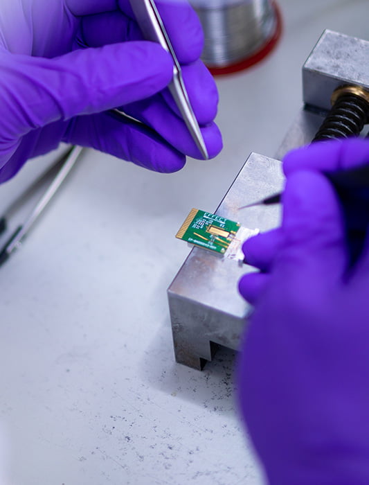
Packaging
PICs are packaged for protection and mounting on a printed circuit board. Photonic chips and electronic chips can be combined in a hybrid module, leveraging the benefits of both: cost reduction and best-in-class processes. It is also possible to configure different combinations of photonic chip types to address the demand for increasingly sophisticated solutions. Our packaging partner PHIX offers assembly services for PICs and other technology platforms, providing housing with electrical connections, optical interfaces, and thermal management.
Applications
With over 20 specialist suppliers, our ecosystem develops components which are serving multiple industries from medical and healthcare, to data and telecom. Through the innovative application of Photonic Integrated Circuits (PICs), companies are creating new solutions to help solve the world’s technological and societal problems.
We can support you in
- Funding for startups
- Subsidising R&D projects
- Grow the talent pool in the industry
- International collaboration