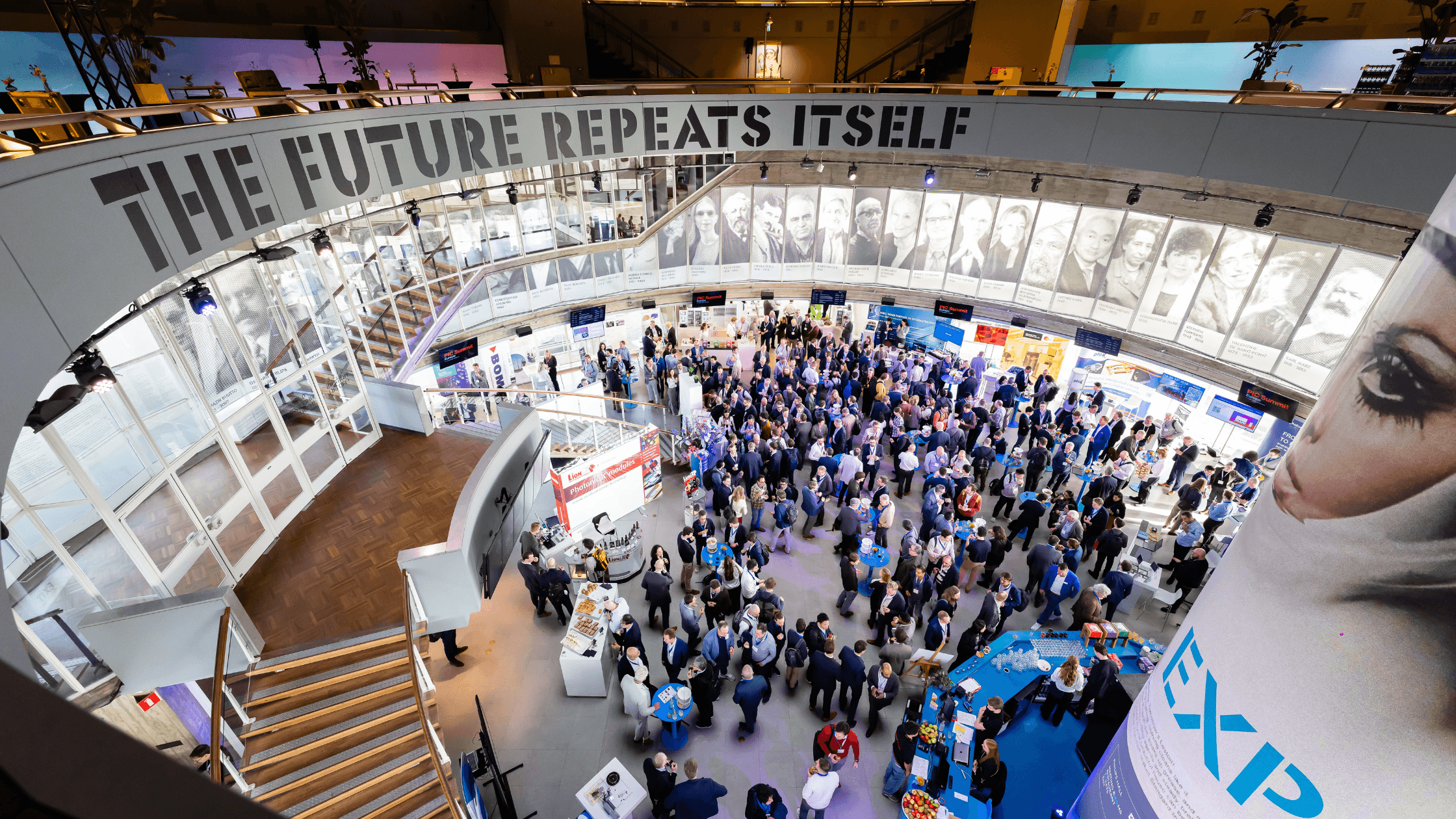
Day 1 Morning Recap: Scaling Together at PIC Summit 2025
04 November 2025PIC Summit 2025 opened with a look back at how far integrated photonics has come and how quickly it’s moving forward. In 2022, the focus was on building a foundation: 1.1 billion euros of funding and the start of a true European community. By 2023, the tone shifted toward geopolitics and jurisdiction, as the sector found itself pulled between global collaboration and regional independence. Last year was all about the need to deliver; to create products, and to go to market. This year, it’s all about AI integration, scalability, and energy efficiency because the world’s data centres are now built on the same light-based technologies this community has been perfecting for years. The challenge now? Balancing cost, quality, and time, all while keeping up with demand.
Moderator Irene Rompa and PhotonDelta CEO Eelko Brinkhoff set the stage: integrated photonics has momentum, but to sustain it, the ecosystem needs funding, supportive legislation, and stronger international partnerships.
Brinkhoff highlighted that PhotonDelta’s Growth Fund Phase 2 will bring €120 million of new investment, a vital boost for Dutch & European companies still fighting to scale despite the need for more policy support. With growing collaboration across Taiwan, Japan, and Singapore, the takeaway is clear: Europe needs to scale together, not in isolation.
Keynote: ASML – Exploring innovations to continue scaling and meet AI demand
Anne Hidma from ASML opened with humility and humour, describing ASML as “a company full of nerds with a good heart”, before diving into how the semiconductor giant sees its own role in the next era of photonics.
ASML’s story started small: a joint venture with Philips, just 31 employees, now Europe’s biggest tech company by market cap with €4 billion in annual R&D. The company’s purpose remains unchanged: harness the power of light. What’s new is the scale, and the speed.
As AI drives demand, chips are everywhere, and soon, AI chips will be everywhere too. Anne compared adoption curves: “It took Facebook four years to reach 100 million users. ChatGPT did it in two months. DeepSeek took one week.” The problem isn’t just innovation; it’s affordability and power. If we keep scaling computing power at this pace, she warned, we’ll need nuclear-level energy just to sustain it. To meet that demand responsibly, ASML focuses on efficiency, 3D integration, and advanced packaging; all of which integrated photonics directly supports.
Anne remarked that scaling takes three key ingredients:
- A strong ecosystem: Close collaboration with customers, partners, and academia.
- A long-term roadmap: Aligning device design with manufacturing timelines.
- Big bets on disruptive tech: Like TWINSCAN, immersion, and EUV once were.
She continued, mentioning integrated photonics is still in the early phase of that journey. The call to action: collaborate across the ecosystem to industrialise integrated photonics and build the tools, standards, and cost structures that make scaling sustainable.
Her closing message resonated clearly: “AI is here. It will fuel demand. Harness light. Scale and innovate together.”
Keynote: Taara – A Success Story of PIC Applications
Next up, Devin Brinkley from Taara: a company spun out of Google X, the “moonshot factory” began by addressing their mission: using light to bring fibre-quality connectivity to places fibre can’t reach.
We’re familiar with the challenge: fibre is fast, but trenching and permits make it slow and expensive to implement. Traditional wireless using radio frequency is easier, but the spectrum is limited. Taara’s answer is the Lightbridge, a compact optical communication unit about the size of a traffic light that consumes the same power as a 40W lightbulb.
Already deployed in over a dozen countries, it’s proven itself in extreme conditions: spanning the Congo River, powering 5G backhaul at Coachella, and providing emergency connectivity in Anguilla after a subsea cable failure. Each unit uses advanced tracking and wavefront correction to maintain alignment, even in tough weather. The next generation will use 2D optical phased arrays to scale up bandwidth and reliability.
Taara’s goal is to become the foundation of high-bandwidth urban networks, serving not just rural connectivity, but also autonomous vehicles, smart cities, and quantum networks.
And like everyone else this morning, Devin connected back to AI: as data and computing power move from massive data centres toward edge devices, photonics and optical communications will keep the world’s AI systems connected, efficient, and scalable.
Keynote: European Commission – The Role of Government in Shaping Integrated Photonics
Almost exactly one year into the new Commission, Gustav Kalbe returned to the stage with a much clearer vision than last year. What was speculation in 2024 has now turned into conviction: integrated photonics is no longer a niche, it’s a strategic priority.
He shared updated projections showing the global integrated photonics market expected to grow from €1.9 billion in 2024 to €7.2 billion by 2031. Europe holds a balanced share across sectors like Industry 4.0, construction materials, and healthcare, but still lags behind in agriculture, food, and large industry applications.
Semivision recently called the Netherlands “the next innovation hub for integrated photonics”; a label the Commission welcomes, though Kalbe emphasised that the ambition is to extend this kind of recognition to all of Europe. His goal is to build a connected, resilient ecosystem that reduces regional chokepoints and dependence on external suppliers.
His comment that the industry remains “at the mercy of the turn of political wind” got a quiet laugh, but the message was serious: policy must be stable and long-term if Europe wants to stay ahead.
Kalbe acknowledged the fragmentation of the European integrated photonics landscape: dominated by SMEs, limited access to finance, and scattered competence centres. Without coordination, he warned that Europe risks losing ground in both market share and strategic autonomy.
Optical communication and interconnects will be essential to maintain Europe’s technological independence, but the Commission’s focus areas are clear:
- Strengthen the EU integrated photonics supply chain
- Build a robust industrial base that resists foreign takeovers
- Expand market share and ensure integrated photonics remain an enabling technology for other critical sectors
Keynote: PIXEurope – A New ChipsJU Pilot Line for PICs.
Valerio Pruneri, ICFO & ICREA Director PIXEurope, brought both humour and authority to the stage, crediting his mother for choosing his career path in engineering; a choice that’s since led to 65 patents and a leading role in building PIXEurope’s new pilot line in Eindhoven.
This marks the fifth pilot line in Europe, bringing together 20 research and technology organisations across 11 countries. Their mission: bridge the “lab-to-fab” gap and create a unified platform for testing, prototyping, and scaling advanced PICs.
PIXEurope focuses on key application areas like communications, cybersecurity, LiDAR (Light Detection and Ranging), AI, and advanced processing. Pruneri emphasised that different applications require different materials and wavelengths, which is why the pilot line will integrate both monolithic and hybrid platforms, from silicon nitride for visible and near-infrared sensing, to indium phosphide and lithium niobate for high-performance optical systems.
Their approach is open access, therefore allowing designers, manufacturers, and vertical integrators to test new designs and prove technology platforms before going into full production. The end goal being proven processes and technology which help industrial partners to scale.
Lastly, Pruneri stressed the importance of synergy between national pilot lines to avoid having to “reinvent the wheel” across countries.
Keynote: Foxconn – Co-Packaged Optics for AI Data Centres
Foxconn’s Dr. Kuo began his presentation by sharing how the company’s “3+3 strategy”: (leveraging resources, mastering cutting-edge tech, and strengthening integration) is fuelling innovation across smart manufacturing, smart cities, and electric vehicles.
His presentation showcased the scale of Foxconn’s involvement from component manufacturing to full AI data centre solutions. A standout line on one of his slides read, “Move over Moore’s Law: Make way for Huang’s Law,” referencing Nvidia’s exponential compute growth.
Foxconn’s Omniverse Digital Twin (FODT) initiative shows how they’re merging integrated photonics to their digital manufacturing workflows. Through meta-holograms and metasurfaces, Foxconn is advancing nanophotonics and silicon photonics across research, academia, and government collaborations.
Long term, Foxconn highlighted indium phosphide as a key enabler for future scalability reducing cost while improving yield. They also anticipate that pluggables will stay relevant for some time, heterogeneous packaging and advanced integration will remain essential, and optical interconnects are the foundation of AI-era data centres.
Keynote: Tower Semiconductors – Nurturing a Dynamic International PIC Foundry Market
Todd Mahlen from Tower Semiconductors was enthusiastic in outlining the challenges and opportunities involved in scaling PIC manufacturing on a global scale.
For Mahlen, the ultimate goal is to lower complexity, cost and power consumption; which means exploring and implementing multiple integration schemes for Integrated Photonics.
Tower’s biggest opportunities lie in LPO (linear packaged optics) and CPO (co-packaged optics). This means providing a robust manufacturing environment, while giving individual companies the flexibility to differentiate and nurture market directions, which remain ongoing challenges. Todd also expressed that building the technology necessary to support these innovative solutions required CapEx-heavy investment.
Outlining the way forward, Todd told delegates that Tower is making a $350 million investment into expanding its global capacity, tripling its ability to produce SiGe (silicon-germanium) and SiPho (silicon phosphide) PICs by mid-2026; to help create a more diverse chip design platform for everything from detachable fibre solutions and LiDAR, to biosensors, quantum computing, and gyroscopes.
In short, the morning centred on one theme: scaling together. From ASML’s deep dive into power and precision to Taara’s approach to connectivity, every talk came back to the same question: How do we keep up with AI’s accelerating demand, ideally sustainably?