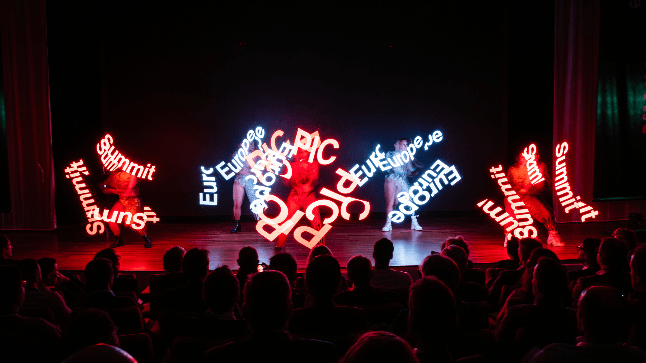
Day 1 Afternoon Recap: Balancing Bottlenecks & Quantum Questions
04 November 2025The second half of PIC Summit Europe 2025 day 1 comprised a mix of keynotes and panel breakout sessions; featuring speakers from international innovators such as imec, as well as new ventures such as Black Semiconductor, who tackled a range of topics from quantum computing to PIC packaging, and everything in between.
Panel: How PICs Accelerate Quantum Tech
This first afternoon session brought together speakers from imec, Quix Quantum, Pixel Photonics, and IonQ to discuss how quantum and integrated photonics are increasingly becoming inseparable. As Gustav Kalbe of the European Innovation Council put it early on, “quantum can’t work without semiconductors, and it can’t work without photonics; they’re vital for each other.”
Daniel De Cruz (IonQ) opened with a quick look at how fast the US quantum market has expanded and gave a synopsis on how IonQ has been building an international presence through their strategic acquisitions and research alliances; all with the goal of positioning itself as the world’s leading quantum companies.
IonQ has already set up a quantum system in Switzerland, an app-development team in Sweden, and an alliance with the Italian government to grow a research and academic ecosystem in the northern part of Italy. IonQ also has a local branch in the UK through its partnership with Oxford Analytics. Excitingly, the company will release its 100 qubit machine later this year and is already working with every major hyperscaler in the US on global use cases.
Next, Stefan Hengesbach (Quix Quantum) took over, saying their vision is simple: “We want to build quantum computers for data centers.” The company is set to deliver its first system to the German Aerospace Center early next year. For Quix, the key enabler is lossless integrated photonics. Their devices aren’t built for one vertical; they’ll have applications across industries, including defense.
Also on their radar? Timing. Hengesbach made a strong case: 90% of market value capture will go to early adopters. He shared an example from a recent automotive manufacturing conference in Stuttgart, asking, “Can you manufacture a car today and be sure it’ll still be quantum-safe in the future?” The answer, for now, is no, and that’s why better integrated photonics platforms and error correction are so critical.
Wladick Hartmann of Pixel Photonics introduced a hardware-level view to the panel. His company focuses on quantum detectors, intentionally staying out of full-stack development to specialise where it counts. As the number of qubits increases, detection becomes a bottleneck, so their approach is to offer one platform with two entry paths: plug-and-play systems and co-integrated detection layers that move research from lab to factory faster.
Panel: Taiwan – Innovation Without Borders
Eelko Brinkhoff, CEO, PhotonDelta, introduced the next panel session, which focused on the technological strides being made in Taiwan.
San-Liang Lee from HiSPA began by outlining the innovation that’s happening on the ground before Chien-Chung Lin (Industrial Technology Research Institute) gave an overview of the Taiwanese Integrated Photonics ecosystem.
He explained more about the work being done at Taiwan’s innovation hub, ITRI, across areas as diverse as smart display, flexible hybrid electronics, and AR/VR before outlining how ITRI is building an ultra-high-speed photonic testing platform capable of 200 GB per second.
“Fast interconnect tech is needed for high bandwidth, low latency data transmissions,” he explained, telling delegates about the progress Taiwan is making in MicroLED and silicon-based solutions.
Panel: Scaling Journeys – Growing Photonics Startups into Global Players
Where’s the money for integrated photonics coming from? What do investors need to know? What’s going to boost their confidence? Innovation or long-term? Who are deep-tech’s investor community?
These were just some of the questions posed to the panel of accomplished investment professionals in the next breakout session.
Wouter Deelman, entrepreneur and founder of ThreeFive Photonics (the first integrated photonics company in the Netherlands), drew from his own experience of raising investment which set his company on a whirlwind trajectory from Delft University to becoming one of the top 50 innovative companies in Europe back in 2000.
“Turning science into a product is a huge mission,” he said. “But after you’ve built the first product that does what it’s supposed to do, the next challenge is finding a customer! Getting funding is a sales process. But that’s something an engineer or scientist doesn’t know how to do. It’s a steep learning curve.”
Rheinhold Voelkel, Co-Chair at the Global Photonics Economic Forum, echoed his sentiments: “Developing micro-optics in a university environment is very different when commercial interest gets involved.”
Steven Konsek, Investment Director at Applied Ventures, explained that good investors prioritise companies with strategic synergies. “For us it starts with identifying what problems you can solve for us and what value you unlock. That’s how we identify high-value problems, that’s where we begin.”
Sujatha Ramanujan, Chief Investment Officer at NextCorps, outlined her experience as an investor, stating that investment isn’t a question of good or bad money, it’s about finding an opportunity that works for you and aligns with your objectives. “Do the homework on where the money’s coming from and what the expectations are,” she advised.
Joachim de Sterke, Co-Founder at PhotonVentures, spoke about his Silicon Valley experience and how getting investment in the US is a lot easier with a prototype; as well as the need to align human capital needs alongside product development and a tech roadmap.
“Investor consortiums; those with multiple shareholders, can mitigate risk for startups,” he said. “More shareholders means a lot more experience to draw from.”
Keynote: Advanced Integrated Photonics Packaging
Azmina Somani (Jabil)’s session jumped straight into the technical realities of packaging photonic and electronic chips at scale. She highlighted how integration is becoming increasingly complex as the industry moves from 2D architectures and beyond, combining PICs and electronic chips within a single stack.
Somani grouped Jabil’s main pain points into three main categories:
- Technical complexity: Optical coupling precision, thermal management, and material compatibility.
- Cost and scalability: Long R&D cycles and high capital expenditure.
- Ecosystem collaboration gaps: Lack of unified design, manufacturing workflows, and talent shortages across disciplines.
Her keynote made one thing clear: standardisation remains their biggest bottleneck. “We need to work on that”, she states. Every vendor’s slight variation in design or process means adapting development methods, repeatedly, across the globe, which adds unnecessary additional time and cost.
She closed by outlining several key factors needed to make mass-scale manufacturing possible:
1. Standardisation, to ensure consistent fibre-coupling and alignment solutions that reduce cost and complexity
2. Vertical integration, or solving the ping-pong problem, where designs bounce between multiple sites and vendors before reaching production
3. Early process definition, using the same tools and recipes to go from prototype to mass production
And 4. Ecosystem cooperation, where foundries, equipment suppliers, and packaging partners work together rather than in silos to anticipate and resolve challenges together.
Keynote: Bottlenecks in Development of Reliable Integrated Graphene Photonics Platform
Cedric Huyghebaert began his keynote by looking back at his early days at imec, where he was one of the first to stack wafers on wafers. Now CTO at Black Semiconductor, he’s working on something equally ambitious: a new way for chips to communicate using graphene photonics.
Since 2009, when graphene and light experiments were first tested, the technology has evolved from basic demonstrations to complex silicon nitride waveguides and damascene contacts.
Graphene has already proven itself in the lab, but the challenge remains making it industrially relevant. The focus now is on connecting it all to electronics using standard industry processes, paving the way for an electronic photonic integrated circuit (EPIC) that combines a graphene modulator and photodetector.
“You can’t just ask a foundry to integrate graphene for you. Or if you can, I’d like to know who said yes.” Huyghebaert said, pointing to the material’s current instability. The goal is to achieve single-crystalline graphene and scale from 200mm to 300mm wafers, using lessons from Complementary Metal-Oxide-Semiconductor (CMOS) manufacturing to improve yield and reproducibility.
Black Semiconductor recently received a €228.7 million grant to build a pilot line for 300mm integrated graphene photonics, moving the technology into production at GlobalFoundries; a major step toward bringing graphene photonics into real-world manufacturing rather than keeping it a lab experiment.
Keynote: Applied Materials Photonics Platform – Catalyzing Photonics for Augmented Reality
Rutger Thijssen took a very different angle, opening his keynote with a cartoon that joked about how hard it used to be for computers to tell if a photo contained a bird. He used it to show how quickly AI has evolved; and how what once needed a research team now fits inside your phone. He argued that the same leap in computational capability is what will drive the next wave of wearable tech: powered by photonics.
He believes that manually typing to an AI chatbot won’t last forever; the future will be visual, contextual, and hands-free: eyewear. Applied Materials aims to use their decades of process know-how to support a new class of smart glasses with integrated displays. “If we do our job well, the technology disappears.” Thijssen continues, “That’s how you create truly human-centric tech.”
Behind each lens sits an entire electronic ecosystem. Therefore, Applied has partnered with GlobalFoundries to manufacture compute boards, sensors, audio components, and connectivity needed to link each pair of glasses to your phone or smartwatch.
Their current reference design, Margarita, weighs just 45 grams and delivers a full-colour field of view. The display assembly is built around a compact lens stack, where the prescription lens and a push lens sandwich the waveguide layer, which is optimised with a light engine for clarity and efficiency.
Thijssen hinted that commercial demand already exists, though NDAs keep launch details quiet.
Panel: The Sweet Spot for Photonic IC Manufacturing Standardisation
Moderator Ivan Nikitski led an open discussion with panelists Michiel Boermans (SMART Photonics), Thomas Hessler (LIGENTEC), and Sander Roosendaal (Synopsys) on what “standardisation” actually means for the photonics industry and where we need to draw the line between efficiency and innovation.
Michiel Boermans said customers are pushing for standards more than ever, especially as foundries scale up. “Tier-1 players know exactly what they want, but SMEs still need guidance,” he said. Too much customization, he warned, creates chaos. “If you have 100 customers and 150 technologies, that just can’t work.”
Thomas added that every foundry needs internal standards and quality frameworks, otherwise you never move beyond the R&D Lab. Deviations should be deliberate, not default.
From a design perspective, Sander Roosendaal argued that standardised design flows accelerate innovation. Compatible software tools, open PDKs, and reusable IP blocks reduce friction and allow designers to move between platforms. He drew parallels with the electronics industry, where shared standards became a foundation for IP exchange and faster development cycles.
When asked how to balance differentiation and scalability, the panelists agreed it’s a trade-off. Customisation has to serve a purpose. “We can’t keep solving one problem with 27 different solutions,” Thomas said. “Standardise the foundation, and then differentiate the product itself.”
Boermans wrapped it up succinctly: understanding both the customer and the foundry will define the key players of the next phase of photonics manufacturing.
Keynote: Shaping the Future of the Photonics Industry with Sustainable Innovation
Patrick Vandenameele, who will step into the role of imec’s next CEO in April 2026, closed the afternoon with a clear reminder that AI is only as powerful as the infrastructure that supports it.
He pointed out the obvious but critical tension in the industry: as compute needs skyrocket, energy consumption climbs with it. To keep scaling responsibly, imec is focusing on improving transistor density, because smaller devices consume less power. But packing billions of transistors into a chip also creates major thermal challenges.
Vandenameele explained that imec’s current priorities include researching low-voltage operation, fine-grained thermal sensing, and new methods for heat dispersion. However memory bandwidth remains a bottleneck; as data has to travel too far between processor and memory, wasting both time and energy.
The next step, he said, is stacking multiple layers of technology, each optimised for a different function, and moving toward 3D chiplet integration. This approach will combine memory, logic, and photonics, making systems faster, smaller, and more efficient.
In short, day 1 revealed a bounty of information shared between key players and industry underdogs. Presenters showcased ample opportunities regarding the future of integrated photonics on a European and global level. Stay tuned to see what day 2 has in store!