The path to future AI data centers is paved with optical interconnect
17 March 2025Today’s generative AI models exceed a trillion parameters, and their computational demands are fast outstripping the computational power of the GPUs, accelerators, and other chips (XPUs) powering hyperscale data centres.
Networking individual XPUs can help bridge this gap. By distributing AI training and inference workloads over many chips, networked XPUs deliver a significantly more powerful and scalable computational platform. Indeed, many envision the future AI data centre as a massive monolithic motherboard integrating thousands, if not millions, of interconnected XPUs.
Only optical I/O interconnect can make this vision a reality, and we look forward to hearing the latest developments at Optica’s OFC 2025 event in San Francisco.
Though conductive copper interconnect is well understood, it presents fundamental limitations when transmitting data signals at the high frequencies required for modern XPUs in the age of AI. As signal frequencies continue to increase, copper’s resistive losses and signal degradation will become even more problematic. Copper traces simply cannot provide the bandwidth, latency, and signal quality to keep up with AI’s demands. Further, its resistive losses convert into heat, which is already fuelling the thermal management issues that are plaguing hyperscale data centres today.
Fibre optic interconnect has long proven its superiority over copper for streamlining bandwidth bottlenecks between data centre servers and switches. Advances in silicon photonics (SiP) have further enabled pluggable optical transceivers to streamline data exchange between racks and boards.
Using light to move data between chips at the board, rack, or system level is the next logical step in this progression. In-package and chip-to-ship optical interconnect not only promise to support the computational bandwidth that AI data centres demand, but they can also reduce latency, heat generation, power consumption, and signal degradation.
The revolution will be digitised
So, why isn’t chip-level optical I/O already widely deployed given its clear benefits? Several hurdles remain to widespread adoption.
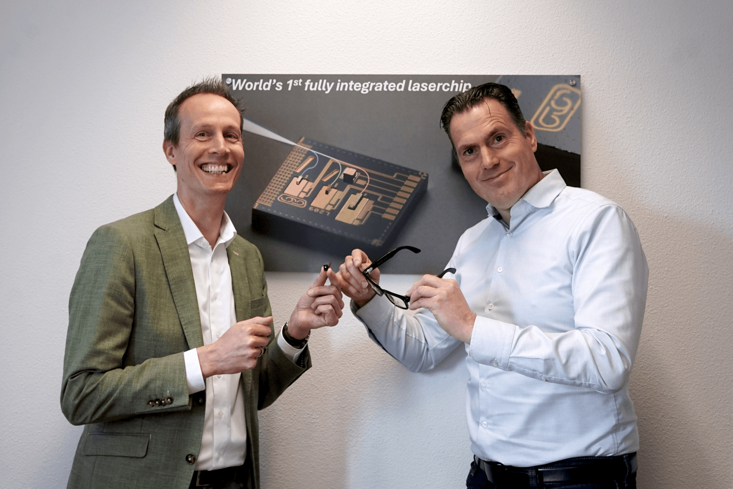
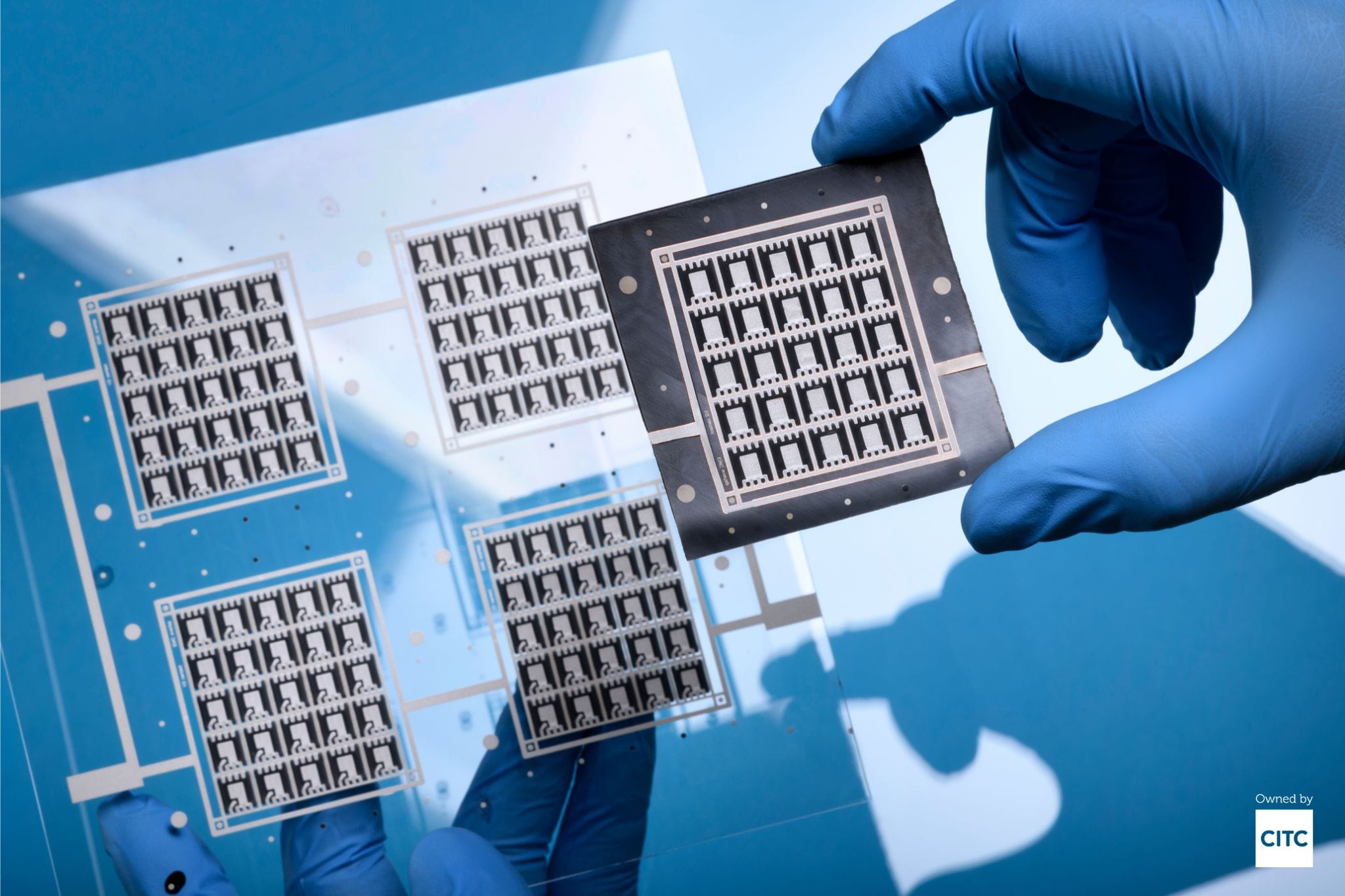
First, optical interconnect introduces manufacturing complexity to decades-old CMOS fabrication processes. Integrating optical components into conventional silicon-based design and fabrication processes demands entirely new design skills, unfamiliar materials, and additional manufacturing steps for both front- and back-end chip-making processes. Such challenges have prompted PhotonDelta companies, SMART Photonics (booth #6067) and EFFECT Photonics (booth #2850), to instead explore alternatives to silicon to integrate photonic functionality in chips used in optical transceivers. This also holds potential for optical I/O.
Second, because optical interconnect is, in some cases, still a relatively unfamiliar technology to chip fabs, producing optical chips at scale without compromising cost or yield on the front end remains a work in progress. On the back end, packaging photonic components requires new and highly precise alignment steps to ensure photonic couplings are optimised. MicroAlign, another PhotonDelta constituent, is tackling this challenge at the chip package level by bringing individual fibre position control to a fibre array. This has helped improve core-based active alignment by 10x without compromising on alignment speed. You can find them at booth #6262.
Lastly, although photons generate far less heat than electrons when carrying high-frequency signals, integrating photonic components such as lasers into the chip package introduces new thermal management considerations to overall chip design.
None of these challenges are insurmountable. Those interested in learning more at OFC 2025 will find ample presentations and exhibitors sharing solutions. When viewed from the perspective of chip foundries that have had decades to refine their CMOS production processes, chip-level optical interconnect represents more of a revolution than an evolution.
Fortunately, the revolution is well advanced and accelerating thanks to the combined efforts of fabs, chipmakers, designers, and industry accelerators like PhotonDelta. Those interested in learning more about optical I/O at OFC 2025 will find many interesting presentations and exhibitors sharing solutions. There are certainly a few industry players that are worth keeping an eye on!
Foundries such as GlobalFoundries (booth #3220), Tower Semiconductor (booth #3322), and TSMC have launched active SiP initiatives to support the fabrication of photonic components as part of their standard CMOS processes. On the chipmaking front, Intel and NVIDIA are investing in next-generation chip-to-chip optical I/O solutions. Intel’s experimental prototypes and NVIDIA’s strategic integration plans underscore the industry’s recognition that optical interconnect is key to unlocking future AI performance.
Chip-to-chip optical I/O cannot scale without the active participation of these industry bellwethers. But many of the biggest innovations are arising from a number of startups worth checking out at OFC 2025.
Among them is Ayar Labs (booth #2958), which recently drew $155 million in Series D funding from semiconductor leaders such as NVIDIA, AMD, and Intel. Ayar’s TeraPHY in-package optical I/O chiplet features a photonic and an electrical integrated circuit as well as other transceiver components to enable bandwidth density up to 2 Tbps per chiplet, or 200 Gbps per millimetre of chip edge. That translates to 1000x the bandwidth density of electrical I/O. TeraPHY’s latency and energy efficiency are both 10x faster than electrical interconnect. Importantly, Ayar Labs’ in-package optical I/O chiplet is fabricated using GlobalFoundries’ 45-nm process.
Lightmatter (booth #5145), which raised $400 million in its recent Series D round, is also working with GlobalFoundries to bring a chip-level optical I/O solution to market, possibly later this year. Lightmatter takes a vertical—or 3D—approach to optical integration by mounting and interconnecting silicon chiplets atop an optical interposer to enable light-speed communications between them.
Celestial AI’s Photonic Fabric aims to support tens of terabytes of optically scalable memory capacity, supporting high-bandwidth memory demands for current and future data centre architectures. Its optical interconnection would link hundreds of GPUs or AI accelerators with industry-leading bandwidth at extremely low latency and energy consumption. You can find them at booth #6441.
Talk to us
The expansion of AI infrastructure has lost none of its momentum as we approach the next OFC event, which explains the deepening investment in chip-level optical interconnect and integrated photonics. PhotonDelta, including 20 of its ecosystem partners, will be on hand at the show to discuss its roadmap for both technologies as well as recent advancements in manufacturability and performance. You can find us at the Holland pavilion located at booth #6165. If you would like to set up a meeting with us, please reach out to office@photondelta.com.