High Tech Campus Eindhoven Invests in, and Constructs Building and Cleanroom Facilities for TNO’s 6-inch Photonic Chip Pilot Line
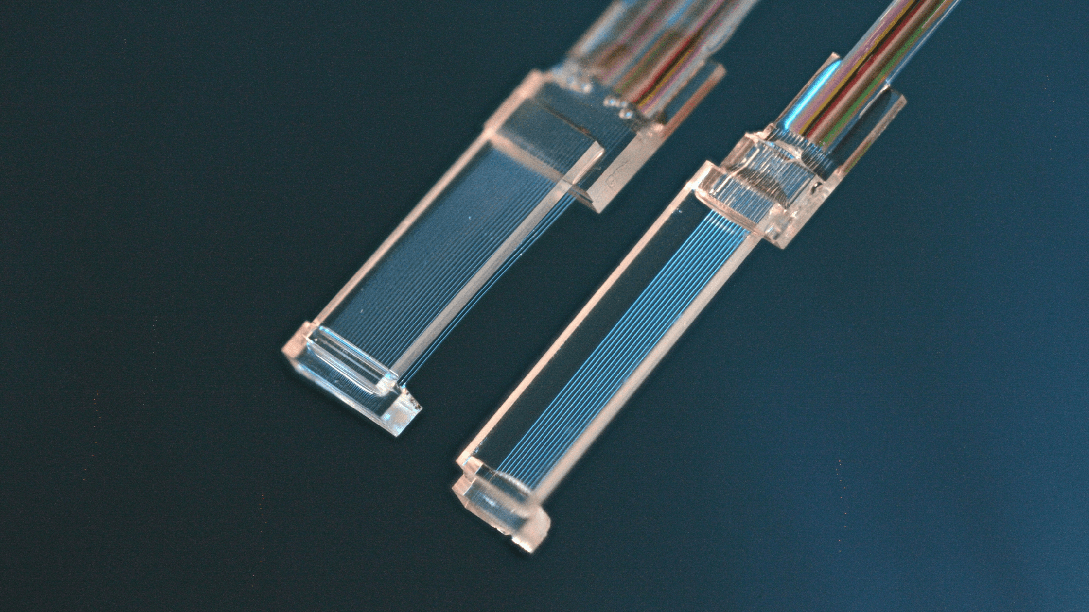
05 November 2025The Netherlands is developing a new industrial pilot line for photonic chips. This pilot line, hosted by TNO and part of the EU’s PIXEurope project, will be built at the High Tech Campus Eindhoven starting in February 2026. Once operational, it will serve as a testbed and fab to facilitate full-scale manufacturing of advanced Indium Phosphide (InP) photonic chips at a 6-inch wafer scale. By combining research and manufacturing, the pilot line will help turn innovative ideas into cutting-edge real-world technologies – faster, energy efficient, more reliable and at scale.
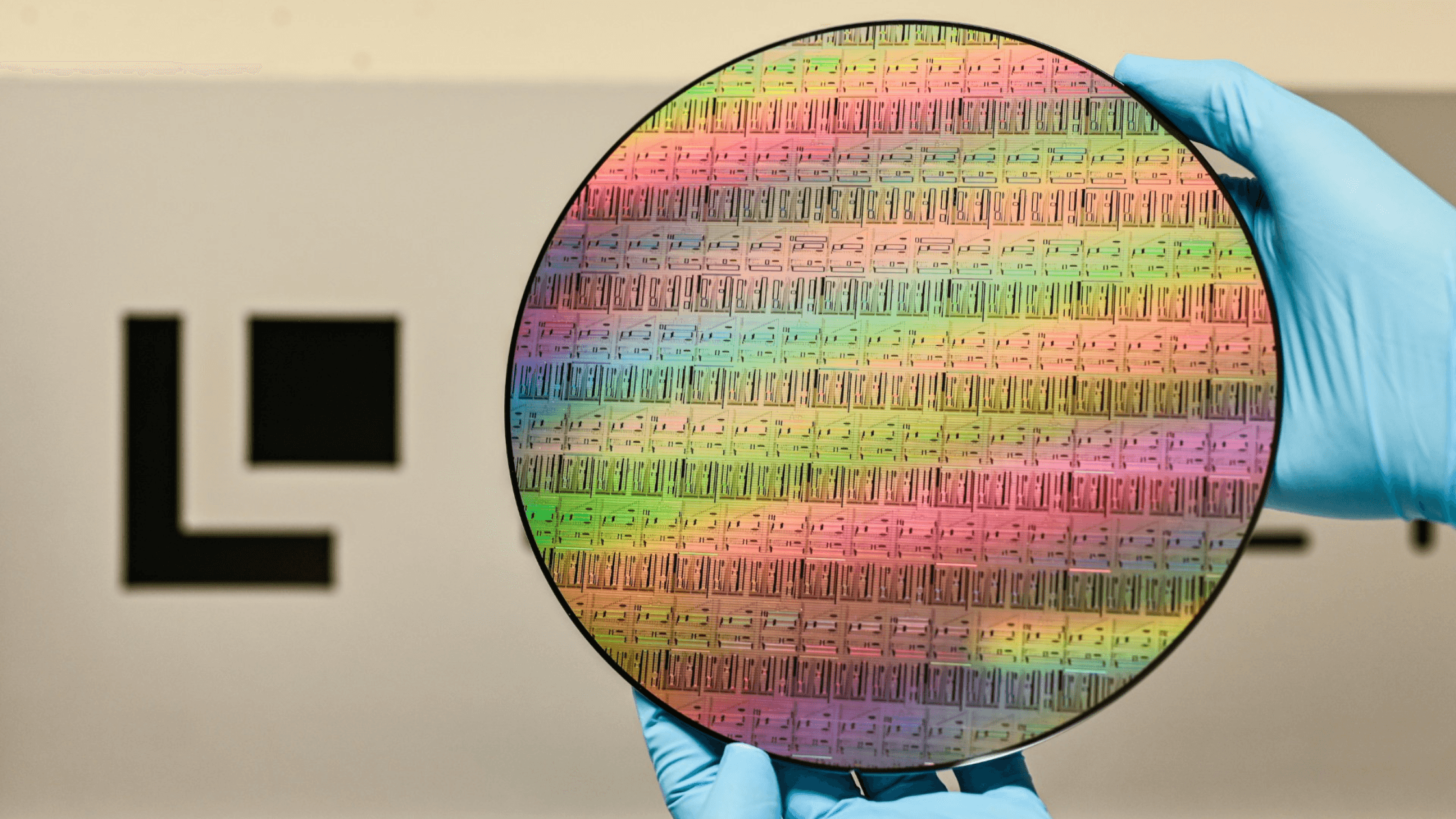
High Tech Campus Eindhoven will provide the building and cleanroom infrastructure for the new pilot line on the north side of the Campus. HTCE is proud to support TNO in enabling the production of integrated photonic chips at scale by investing in and constructing the facilities required. The facility will focus on 6-inch wafers, a larger wafer size that allows higher efficiency and greater throughput, with the goal of producing up to 10,000 wafers per year. This step represents an important move toward industrial-scale manufacturing of photonic chips in the Netherlands and Europe.
Ton van Mol, Managing Director at TNO: “This photonic chip pilot line is a game-changer for Dutch companies and the future earning power and prosperity for the Netherlands. It is a critical part of a powerful PhotonDelta ecosystem with which the Netherlands can distinguish itself worldwide.”
HTCE invests as a partner in projects that are of strategic importance to its tenants, the region, and the future earning capacity of the Netherlands. Providing technical facilities and infrastructure, and offering an inspiring place to work on the smartest square kilometre in Europe, is at the core of what HTCE does. These investments are continuously expanded to enable companies to innovate and grow faster.
Otto van den Boogaard, CEO of High Tech Campus Eindhoven: “Our mission as High Tech Campus Eindhoven is to support companies and institutes that develop cutting-edge technologies. We were asked to invest in and provide the building and cleanroom for this pilot line. We are proud and excited to step in as a partner in this initiative. Together, we strengthen our position as the home base for breakthrough technology and innovation.”
PhotonDelta ecosystem
The pilot line is a joint effort by leading Dutch organisations. Startups, SMEs, and established companies will use the facility to develop and scale up their products in the InP photonic chip domain.
Eelko Brinkhoff, CEO PhotonDelta: “In 2027 this state-of-the-art facility houses one of the most advanced integrated photonics pilot lines in the world. The goal is simple: take photonics chip technology from lab to fab. This fab will create a unique infrastructure for companies to have their prototypes developed, offering a solution to challenges in, for example, datacom, healthcare and the automotive industry.”
As a European leader in InP technology, SMART Photonics is, next to others, an important knowledge provider and end user of the pilot line, while also serving as a training provider to help build the skills and knowledge needed across the ecosystem.
Johan Feenstra, CEO SMART Photonics: “We are thrilled to engage in this much-needed ecosystem initiative, which will strengthen our ability to serve our customers in all markets even better. By scaling up together, we ensure this collaboration strengthens our leading position in the Netherlands and across Europe.”
PIXEurope: a European initiative
PIXEurope is a European programme under the Chips Joint Undertaking (Chips JU). Its long-term goal is to establish the world’s first fully integrated, open-access pilot line for photonic chips in Europe. The Eindhoven pilot line is part of PIXEurope and is funded through the EU Chips Act, PhotonDelta, TNO, and the Dutch Ministries of Economic Affairs and Defence.
PIXEurope brings together leading research organisations and industrial partners to address key technological and production challenges across the entire photonic chip supply chain, including advanced chip fabrication, materials integration, packaging, and testing. The programme also supports the integration of photonic and electronic circuits, paving the way for next-generation semiconductor systems and strengthening Europe’s position in this critical technology field.