Manufacturing yield rates represent one of the most critical metrics in photonic chip production, directly affecting both cost-effectiveness and scalability. As integrated photonics moves toward industrial-scale manufacturing, understanding yield performance becomes essential for companies evaluating production feasibility and investment decisions.
The PhotonDelta ecosystem has been actively addressing yield optimization across different photonic chip platforms, including indium phosphide (InP), silicon nitride (SiN), and silicon photonics (SiPh). With growing demand for photonic integrated circuits (PICs) expected to reach 300 million units by 2030, yield improvements are fundamental to meeting market requirements while maintaining competitive pricing.
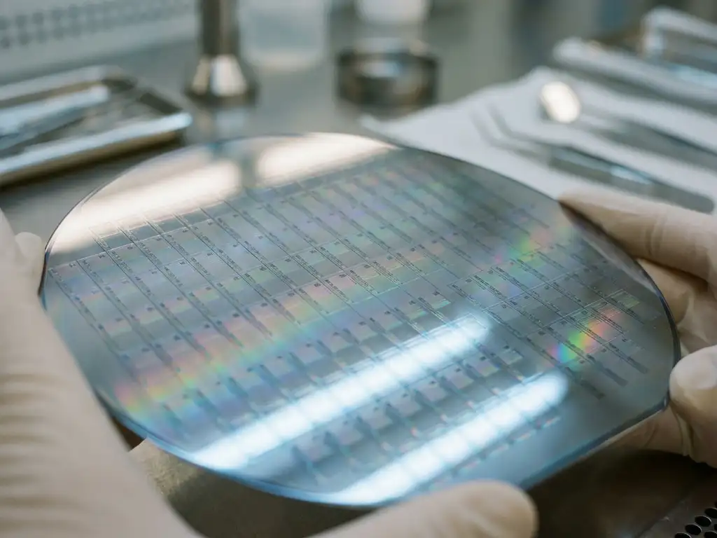
What is yield rate in photonic chip manufacturing?
Yield rate in photonic chip manufacturing refers to the percentage of functional chips produced from a wafer that meet specified performance criteria. This metric measures how many chips pass all optical, electrical, and packaging tests compared with the total number of chips fabricated on each wafer.
Manufacturing yield encompasses multiple stages of the integrated photonics value chain. During wafer fabrication, yield depends on the precision of lithographic processes, material quality, and contamination control. Complexity increases for photonic chips because they must maintain both optical and electrical functionality simultaneously.
Yield calculations typically consider die-level functionality, where each individual chip must demonstrate proper light coupling, signal transmission, and integration with electronic components. Unlike purely electronic semiconductors, photonic chips require additional testing for optical loss, wavelength accuracy, and polarization characteristics. The PhotonDelta ecosystem addresses these challenges through standardized testing protocols across its foundry partners.
What are typical yield rates for photonic chips?
Typical yield rates for photonic chips currently range from 30% to 70%, depending on the platform, complexity, and manufacturing maturity. Silicon nitride platforms often achieve higher yields due to their compatibility with established CMOS processes, while indium phosphide yields vary more significantly because of wafer-size limitations and material properties.
Production volumes significantly influence yield performance. Multi-Project Wafer (MPW) runs, commonly used in the PhotonDelta ecosystem for cost-effective prototyping, typically show lower yields than dedicated production runs. This occurs because MPW processes optimize for flexibility rather than yield maximization.
Platform-specific yield characteristics reflect material properties and processing requirements. Silicon photonics benefits from mature semiconductor manufacturing infrastructure, often achieving yields comparable to those of electronic chips in high-volume production. However, the need to integrate light sources can reduce overall system yield. Indium phosphide platforms face yield challenges due to the brittle nature of the material, which limits wafer sizes and increases handling complexity.
What factors affect photonic chip manufacturing yield?
Manufacturing yield in photonic chips is primarily affected by optical coupling efficiency, material defects, lithographic precision, and integration complexity. Process variations that might be acceptable in electronic chips can cause significant optical loss or wavelength shifts in photonic devices.
Material quality is a fundamental yield factor. Silicon nitride platforms benefit from abundant silicon availability and established processing techniques, contributing to more predictable yields. Indium phosphide faces inherent challenges due to material brittleness and higher costs, which limit wafer sizes and increase sensitivity to defects.
Design complexity significantly affects yield rates. Simple passive photonic circuits typically achieve higher yields than active devices that require precise light-source integration. The PhotonDelta ecosystem addresses this through its design library, which provides tested building blocks that reduce design-related yield losses.
Environmental factors during fabrication, including temperature control, vibration isolation, and contamination prevention, critically affect photonic chip yield. Even minor particles can disrupt optical waveguides, while temperature variations can cause wavelength drift beyond specification limits.
How does photonic chip yield compare to electronic semiconductor yield?
Photonic chip yields are generally lower than mature electronic semiconductor yields, which often exceed 90% in high-volume production. This difference stems from the dual optical-electrical functionality requirements and the relative manufacturing maturity of the two industries.
Electronic semiconductors benefit from decades of process optimization and standardization. The semiconductor industry has developed sophisticated yield-enhancement techniques, defect-reduction strategies, and statistical process control methods. Integrated photonics manufacturing is following a similar trajectory but remains at an earlier stage of development.
Testing complexity contributes to yield differences. Electronic chips primarily require electrical testing, while photonic chips need both electrical and optical characterization. This dual testing requirement can reveal additional failure modes and reduce apparent yield rates.
The PhotonDelta ecosystem recognizes this maturity gap and works to accelerate yield improvements through shared best practices, standardized processes, and collaborative development programs across its foundry partners.
How can manufacturers improve photonic chip yield rates?
Manufacturers can improve photonic chip yield rates through design optimization, process standardization, advanced metrology, and statistical process control. The most effective approach combines design-for-manufacturing principles with systematic process improvements and real-time monitoring.
Design optimization focuses on using proven building blocks and avoiding unnecessary complexity. The PhotonDelta ecosystem supports this through its comprehensive design library, which provides pre-tested components that reduce design-related yield losses. Standardized design rules help ensure manufacturability across different foundry partners.
Process improvements target critical control points in fabrication. This includes enhanced lithography control for precise waveguide dimensions, improved material-deposition uniformity, and better contamination control throughout the manufacturing process. Regular calibration and maintenance of fabrication equipment help maintain consistent performance.
Advanced packaging techniques can recover some chips that fail initial testing. Hybrid integration approaches, in which photonic and electronic components are combined at the module level, provide flexibility to optimize individual component yields separately. This strategy allows manufacturers to achieve higher system-level functionality even with moderate chip-level yields.
As the photonic industry continues to mature, yield optimization remains a collaborative effort that extends beyond individual manufacturing facilities. Companies looking to advance their photonic chips development often benefit from participating in broader industry initiatives that share knowledge and resources. The integrated photonics ecosystem thrives when manufacturers, researchers, and technology developers work together to address common challenges. Organizations seeking to build expertise in this field typically focus on developing specialized human capital while exploring various funding opportunities to support their yield improvement initiatives. Through continued investment in process development and internationalisation of best practices, the photonic manufacturing industry is steadily moving toward the yield rates necessary for widespread commercial adoption.