Photonic chips represent a significant advancement in semiconductor technology, using photons instead of electrons to process and transmit information. However, these sophisticated devices face unique manufacturing challenges that differ substantially from those of traditional electronic semiconductors. Understanding how environmental contaminants affect integrated photonics is crucial for anyone considering investment or partnership opportunities in this rapidly growing sector.
The sensitivity of photonic chip technology to dust contamination directly affects manufacturing costs, yield rates, and overall production scalability. For international companies evaluating the Dutch integrated photonics ecosystem, these manufacturing requirements play a critical role in facility planning and operational decision-making.
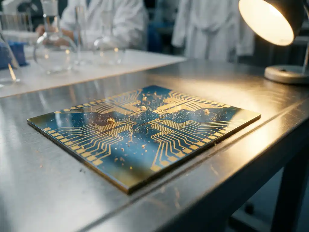
What Happens When Dust Particles Land on Photonic Chips?
When dust particles land on photonic chips, they can scatter or block light signals traveling through the chip’s waveguides, causing immediate signal loss and degraded performance. Unlike electronic chips that rely on electrical current, photonic integrated circuits (PICs) depend on precise light transmission through microscopic pathways, making even tiny contaminants problematic.
The impact varies depending on where contamination occurs during the manufacturing process. Dust particles that settle on waveguide surfaces create optical losses by disrupting the carefully engineered refractive-index differences that guide light through the chip. These particles can also cause unwanted reflections, sending light signals in unintended directions and creating crosstalk between different optical channels.
During fabrication, dust contamination can permanently damage a chip’s optical properties. Particles that become embedded in photonic structures during material deposition or etching create defects that cannot be easily corrected. This contamination directly affects manufacturing yield, making cleanroom protocols essential for the cost-effective production of photonic chips.
Why Are Photonic Chips More Sensitive to Dust Than Electronic Chips?
Photonic chips are more sensitive to dust than electronic chips because they rely on precise optical interactions that operate at wavelength scales, typically 1–2 micrometers. Any particle approaching these dimensions can significantly disrupt light propagation, whereas electronic chips can often function despite similar contamination levels affecting their larger electrical pathways.
The fundamental difference lies in how these technologies operate. Electronic chips use electrical current that can often route around small obstructions or contamination. In contrast, integrated photonics requires unobstructed light paths through waveguides with tolerances measured in nanometers. Even submicron dust particles can cause measurable optical losses or complete signal blockage.
Additionally, photonic chips often incorporate multiple material platforms, such as silicon nitride, indium phosphide, and silicon photonics, each with specific surface requirements. These different materials may react differently to contamination, with some platforms showing greater sensitivity to particular types of particles. Optical coupling between different components on a single chip also creates multiple points where dust contamination can disrupt system performance.
How Does Dust Contamination Affect Photonic Chip Performance?
Dust contamination affects photonic chip performance by increasing optical losses, reducing signal quality, and creating unwanted interference between optical channels. These effects directly translate to reduced data transmission speeds, higher error rates, and decreased overall system efficiency in applications ranging from telecommunications to sensing.
Performance degradation manifests in several specific ways. Signal attenuation occurs when dust particles absorb or scatter light passing through waveguides, requiring higher input power to maintain the desired output levels. This increased power requirement reduces the energy-efficiency advantages that make photonic chip technology attractive for data centers and telecommunications applications.
Contamination also affects the precision-sensing capabilities that make PICs valuable in medical and automotive applications. In biosensing applications, where photonic chips detect minute changes in optical properties, dust particles can create false signals or mask genuine biological responses. For automotive LiDAR applications, contamination can reduce the accuracy of distance measurements that are critical for autonomous-vehicle safety systems.
Crosstalk between optical channels represents another significant performance impact. When dust particles cause light to scatter from one waveguide into adjacent channels, they create interference that degrades signal integrity across the entire chip. This effect is particularly problematic in high-density photonic circuits designed for advanced telecommunications applications.
What Cleanroom Standards Are Required for Photonic Chip Manufacturing?
Photonic chip manufacturing typically requires ISO Class 1 to Class 10 cleanroom standards, which limit particles larger than 0.1 micrometers to fewer than 10–100 particles per cubic foot of air. These stringent requirements exceed those of many electronic chip manufacturing standards due to the optical sensitivity of integrated photonics.
The specific cleanroom classification depends on the manufacturing step and the photonic platform being used. Critical processes such as waveguide formation and optical coupling require the most stringent Class 1 conditions, while packaging and testing operations may function adequately in Class 10 environments. The PhotonDelta ecosystem maintains these standards across its integrated photonics value chain, ensuring consistent quality for both research and production activities.
Beyond particle-count limits, photonic chip manufacturing requires specialized contamination-control measures. Temperature and humidity control are critical because thermal fluctuations can affect the optical properties of photonic materials. Vibration isolation is also essential, as mechanical disturbances during fabrication can create surface irregularities that scatter light.
Personnel protocols in photonic cleanrooms often exceed standard semiconductor requirements. Workers must use specialized garments that minimize particle generation, and entry procedures include additional decontamination steps. The manufacturing equipment itself requires frequent cleaning and calibration to maintain the optical precision necessary for reliable photonic chip production. These enhanced protocols contribute to the overall cost structure of photonic chip manufacturing but remain essential for achieving the performance levels required by demanding applications in telecommunications, healthcare, and automotive sectors.
As the photonic industry continues to mature, understanding these contamination challenges becomes increasingly important for companies navigating this complex landscape. The specialized manufacturing requirements we’ve discussed highlight why photonic chips demand such careful attention to environmental controls throughout production. For organizations considering entry into this field, the stringent cleanroom standards and contamination-control measures represent both challenges and opportunities within the broader ecosystem. Companies looking to build expertise in this area will find that developing the right human capital is essential for mastering these manufacturing complexities. The investment in proper contamination control, while substantial, opens doors to internationalisation opportunities as global demand for high-performance photonic solutions continues to grow. Whether you’re exploring partnership opportunities or seeking funding for photonic ventures, understanding these fundamental manufacturing requirements provides the foundation for making informed strategic decisions in this rapidly evolving field.