Photonic chips face several significant disadvantages that can limit their widespread adoption and implementation. These challenges include technical limitations, higher manufacturing costs, complex production requirements, environmental sensitivities, and talent shortages. Despite their promising applications in telecommunications, healthcare, and the automotive industry, these disadvantages currently restrict their market penetration compared to traditional electronic semiconductors.
What are the main technical limitations of photonic chips?
Photonic chips encounter substantial technical challenges that affect their functionality and integration capabilities. Manufacturing precision requirements demand extremely tight tolerances, often at nanometer levels, making consistent production difficult. Integration complexity with electronic systems creates significant hurdles, since photonic and electronic components operate on fundamentally different principles: light versus electrons.
Power consumption presents another limitation for certain applications. While photonic chips excel in data transmission efficiency, some implementations require substantial electrical power for driving lasers and maintaining optical components. Wavelength-dependent performance variations also affect reliability, as different wavelengths can behave differently within the same chip architecture.
Platform-specific constraints further complicate development. For instance, silicon photonics (SiPh) platforms need integrated light sources and experience higher propagation loss compared to silicon nitride (SiN). Meanwhile, indium phosphide (InP) suffers from higher propagation losses and material brittleness that limits wafer size. These platform limitations often require hybrid solutions, increasing complexity and development time.
Why are photonic chips more expensive than traditional electronic chips?
Photonic chips cost significantly more than traditional electronic semiconductors due to specialized manufacturing processes and limited production volumes. Material costs contribute substantially, particularly for InP platforms, where indium is an expensive and brittle material compared to the abundant silicon used in conventional chips.
The specialized fabrication equipment required for photonic chip production demands substantial capital investment. Unlike electronic chip manufacturing, which benefits from decades of infrastructure development, photonic chip foundries require unique optical testing capabilities and precision alignment equipment. This specialized tooling cannot fully leverage existing semiconductor manufacturing economies of scale.
Limited production volumes prevent manufacturers from achieving the cost efficiencies available in traditional semiconductor production. The electronic chip industry produces over 1 trillion units annually, while the photonic chip market remains in its infancy with significantly lower volumes. Complex testing requirements add further costs, as photonic chips need both electrical and optical characterization throughout the manufacturing process.
The current lack of mature supply chain infrastructure compounds cost challenges. Unlike established semiconductor manufacturing with well-developed supplier networks, photonic chip production relies on specialized vendors with limited competition, resulting in higher component and service costs.
What manufacturing challenges make photonic chips difficult to produce?
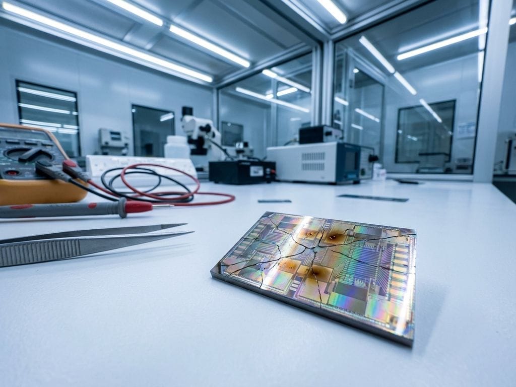
Manufacturing photonic chips presents unique production complexities that exceed those found in traditional semiconductor fabrication. Extremely tight tolerance requirements demand precision at the subwavelength level, typically requiring accuracy within tens of nanometers for optical waveguides and coupling structures.
Specialized fabrication equipment needs create significant barriers to entry. Photonic chip production requires tools capable of precise optical lithography, specialized etching processes for waveguide formation, and unique deposition techniques for optical materials. These tools often lack the maturity and availability of conventional semiconductor equipment.
Yield optimization presents ongoing difficulties due to the sensitivity of optical components to manufacturing variations. Small deviations in layer thickness, surface roughness, or alignment can dramatically affect optical performance, making consistent high-yield production challenging. Quality control requires sophisticated optical testing at multiple production stages, adding complexity and time to manufacturing processes.
Cleanroom environments need specific optical testing capabilities beyond standard semiconductor requirements. Multi-project wafer (MPW) runs, while cost-effective for prototyping, limit design complexity and production flexibility. The requirement for different platform expertise—InP, SiN, and SiPh—means foundries must maintain multiple specialized process lines rather than standardizing on a single manufacturing approach.
How do environmental factors affect photonic chip performance?
Environmental factors significantly impact photonic chip performance due to the sensitive nature of optical components and light-based operations. Temperature fluctuations affect optical properties by changing the refractive indices of materials, shifting wavelength responses, and altering the performance of active components like lasers and photodetectors.
Humidity effects on materials can cause dimensional changes in packaging materials and affect the performance of optical coatings. Moisture ingress can lead to degradation of optical interfaces and changes in material properties that affect light transmission. Mechanical stress sensitivity presents challenges, as physical deformation can misalign optical components and alter waveguide properties.
The aging characteristics of optical components differ from those of electronic semiconductors, with lasers experiencing gradual power degradation and optical materials potentially developing defects over time. These aging effects can shift performance parameters and require different reliability considerations compared to traditional electronic chips.
Packaging challenges for environmental protection become critical, since photonic chips often require optical input/output connections that can create potential ingress points for contaminants. The packaging must maintain optical alignment while providing environmental sealing, creating design trade-offs between performance and protection. Thermal management becomes more complex as both electrical and optical components generate heat, requiring specialized cooling solutions that maintain optical alignment.
What are the current skill gaps and talent shortages in photonic chip development?
The photonic chip industry faces significant workforce challenges due to the specialized knowledge required to combine optics and electronics expertise. Cross-disciplinary skills in photonics, materials science, and semiconductor processing remain scarce, as traditional educational programs typically focus on either electronics or optics separately rather than integrated approaches.
Limited educational programs specifically addressing integrated photonics create a pipeline shortage of qualified engineers. Most universities offer either electrical engineering or optical engineering degrees, but few provide comprehensive training in photonic integrated circuits. This educational gap means professionals must develop expertise through on-the-job training, slowing industry growth.
The shortage of experienced engineers compounds development challenges, as photonic chip design requires an understanding of both optical physics and semiconductor manufacturing processes. Engineers need expertise in areas including optical design software, cleanroom processes, packaging techniques, and testing methodologies specific to photonic devices.
Industry growth projections suggest these talent shortages will intensify as demand increases. The PhotonDelta ecosystem aims to create 85,000 jobs by 2030, but current educational capacity cannot meet this demand without significant program expansion. Companies must invest heavily in training programs and partnerships with universities to develop the necessary workforce, adding costs and time to technology development initiatives.
While these challenges may seem daunting, the photonic chip industry continues to evolve through collaborative approaches that address each limitation systematically. The growing ecosystem of companies, research institutions, and government organizations is working together to tackle manufacturing complexities and cost barriers. Strategic funding initiatives help bridge the gap between research and commercial viability, while dedicated human capital development programs are expanding the skilled workforce needed for this specialized field. As photonic chips continue to demonstrate their potential across diverse applications, ongoing internationalization efforts are creating the global partnerships necessary to overcome these technical and economic hurdles, paving the way for broader adoption of this transformative technology.