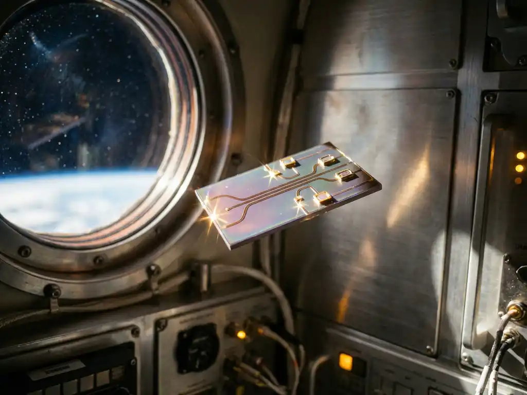
Space exploration demands technology that can withstand the harshest conditions imaginable, from extreme temperatures to intense radiation. As satellites, space stations, and deep-space missions become more sophisticated, the need for reliable communication and sensing systems has never been greater. Photonic chips, which use light instead of electrons to process information, are emerging as a critical solution for space applications where traditional electronics often fail.
The unique properties of integrated photonics make this technology particularly well suited to the demanding environment of space. Unlike conventional electronic systems, photonic chip technology offers inherent resistance to radiation damage while maintaining the high-speed data-transmission capabilities essential for modern space missions.
What Are Photonic Chips and Why Are They Used in Space?
Photonic chips are photonic integrated circuits (PICs) that use light particles (photons) instead of electrons to transmit, process, and manipulate information on a single semiconductor substrate. In space applications, these chips provide high-speed data transmission, reduced power consumption, and enhanced resistance to radiation compared with traditional electronic systems.
The core advantages that make photonic chip technology ideal for space environments stem from the fundamental physics of light-based processing. Photons are not affected by electromagnetic interference in the same way electrons are, making photonic systems naturally more stable in the electrically noisy environment of space. Additionally, the compact, scalable design of integrated photonics allows multiple optical components to be manufactured on a single chip, reducing the overall size and weight of space-bound equipment.
Space missions rely heavily on communication systems that must maintain reliable data links across vast distances. The reduced signal loss and interference characteristics of photonic chips help ensure that critical mission data reaches Earth with minimal degradation. Furthermore, the ability to scale these systems to high volumes at low cost makes them economically viable for both government space agencies and commercial satellite operators.
How Do Space Conditions Affect Photonic Chip Performance?
Space conditions, including extreme temperature fluctuations, vacuum environments, and high-energy radiation, can impact photonic chip performance, but these effects are generally less severe than their impact on traditional electronics. The primary concerns are thermal expansion in optical components and potential radiation-induced changes in optical materials over extended mission durations.
Temperature variations in space can range from extremely cold in shadowed regions to intensely hot when exposed to direct solar radiation. These thermal cycles can cause mechanical stress in photonic components, potentially affecting the precise alignment required for optimal light transmission. However, modern photonic chip designs incorporate thermal-compensation techniques and use materials with matched thermal-expansion coefficients to minimize these effects.
The vacuum environment of space actually benefits photonic systems in some ways, as it eliminates atmospheric absorption and scattering that can degrade optical signals on Earth. The absence of moisture and atmospheric contaminants also reduces the risk of optical surface degradation over time. This makes space an ideal operating environment for the high-speed data-transmission capabilities that define integrated photonics as a key enabling technology.
What Makes Photonic Chips Radiation Tolerant Compared to Electronics?
Photonic chips demonstrate superior radiation tolerance because photons, unlike electrons, are not directly affected by ionizing radiation. While radiation can still damage the semiconductor materials that guide and manipulate light, the optical signals themselves remain largely unaffected by the high-energy particles common in space environments.
Traditional electronic circuits suffer from radiation-induced effects such as single-event upsets, where cosmic rays flip individual bits in memory, and total ionizing dose effects that gradually degrade semiconductor performance. In contrast, photonic systems process information using light signals that pass through waveguides, making them inherently less susceptible to these radiation-induced errors.
The materials used in photonic chip technology, particularly silicon nitride (SiN) and silicon photonics (SiPh) platforms, show excellent stability under radiation exposure. SiN-based systems offer low-propagation-loss waveguides that maintain their optical properties even after extended radiation exposure. While some radiation-induced changes can occur in the semiconductor substrate over very long periods, these typically have minimal impact on the optical signal quality and transmission characteristics that are critical for space applications.
Which Space Applications Benefit Most from Photonic Technology?
Satellite communication systems, space-based LiDAR for planetary mapping, and high-speed data links between spacecraft and ground stations benefit most from photonic technology. These applications leverage the high-speed data transmission, reduced power consumption, and compact design advantages that integrated photonics provides.
Optical transceivers for space-based data communications represent one of the most immediate applications. These systems enable high-speed data transfer for both short-range communication between spacecraft components and long-range transmission back to Earth. The energy-efficient nature of photonic chips is particularly valuable in space, where power generation is limited and every watt must be carefully managed.
Advanced sensing applications also show tremendous promise. Space-based LiDAR systems using photonic chip technology can create precise 3D maps of planetary surfaces, asteroid compositions, and atmospheric conditions. The compact, lightweight nature of photonic sensors makes them ideal for missions where payload weight and volume are critical constraints.
Quantum communication systems for secure space-to-ground links represent an emerging application area. The PhotonDelta ecosystem’s research into quantum photonic applications positions integrated photonics as essential for next-generation secure communication networks that span Earth and space-based platforms.
How Are Photonic Chips Tested for Space Readiness?
Photonic chips undergo rigorous qualification testing, including radiation exposure tests, thermal cycling, vibration testing, and vacuum-chamber validation, to ensure they meet space-mission requirements. These tests simulate the harsh conditions of launch and long-term space operation to verify performance and reliability.
Radiation testing involves exposing photonic components to high-energy particles and gamma radiation at levels that exceed expected mission doses. This testing validates that the optical properties of waveguides and other photonic elements remain stable throughout the mission lifetime. The integrated photonics value chain includes specialized facilities that can perform these critical qualification tests.
Thermal qualification testing subjects photonic chips to repeated temperature cycles that simulate the extreme variations experienced in space. Components must demonstrate consistent optical performance across temperature ranges that can span several hundred degrees. Additionally, mechanical testing, including vibration and shock tests, ensures that the precise optical alignments required for photonic systems remain intact during launch and deployment.
The comprehensive testing approach developed within the European integrated photonics ecosystem helps strengthen Europe’s position in space-qualified photonic systems. This testing capability, combined with the end-to-end manufacturing and design expertise available through organizations like PhotonDelta, positions the region as a key supplier of space-ready photonic solutions for both European and international space missions.
As space missions continue to push the boundaries of what’s possible, the role of photonic chips in enabling these advances becomes increasingly clear. The convergence of radiation tolerance, energy efficiency, and high-speed performance makes this technology indispensable for next-generation space applications. For organizations looking to enter this growing market, understanding the complex interplay between materials science, optical engineering, and space qualification requirements is essential. The collaborative nature of developing space-grade photonic systems often requires expertise from across the entire ecosystem, from research institutions to specialized manufacturers. As commercial space ventures expand and government missions become more ambitious, the demand for skilled professionals in this field continues to grow, highlighting the importance of human capital development in photonics. The success of European companies in this sector also demonstrates how strategic funding and internationalisation efforts can position entire regions at the forefront of transformative technologies that will define the future of space exploration.