Photonic chip manufacturing involves creating photonic integrated circuits (PICs) that use light instead of electrons for data processing. The process requires specialised materials such as silicon, indium phosphide, and silicon nitride, along with precise fabrication techniques including lithography, etching, and deposition. Manufacturing facilities need dedicated equipment for optical alignment and testing, while scaling production faces challenges in yield optimisation and standardisation across the integrated photonics value chain.
What are photonic chips and how do they differ from electronic chips?
Photonic chips, also known as photonic integrated circuits (PICs), are microchips that process information using light (photons) instead of electrical charge carriers (electrons). Unlike traditional electronic semiconductors that rely on electrical current flow, photonic chips manipulate light signals through waveguides, modulators, and other optical components integrated onto a single substrate.
The fundamental difference lies in their operating principles. Electronic chips control electron flow through transistors and conductive pathways, while photonic chips guide and manipulate light through optical waveguides and photonic components. This distinction creates unique manufacturing requirements, as photonic devices need precise optical alignment and materials with specific refractive indices.
Photonic chips offer several advantages over their electronic counterparts, including higher bandwidth capacity, reduced power consumption for data transmission, and immunity to electromagnetic interference. However, they require different manufacturing approaches, particularly in substrate preparation, waveguide fabrication, and optical coupling processes that do not exist in traditional semiconductor production.
What are the main steps in photonic chip manufacturing?
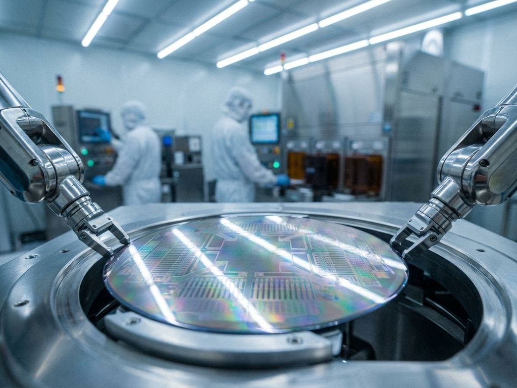
Photonic chip manufacturing follows a systematic process beginning with substrate preparation and ending with comprehensive optical testing. The complete manufacturing workflow includes wafer fabrication, lithography patterning, etching processes, material deposition, and final integration steps that create functional optical circuits.
The process starts with substrate preparation, where materials such as silicon, indium phosphide, or silicon nitride wafers are cleaned and prepared for processing. Epitaxial growth may be required for certain platforms, particularly indium phosphide PICs, where multiple layers are grown with precise thickness and composition control.
Lithography follows, using electron-beam or optical lithography to pattern the photonic circuit designs onto the substrate. This step requires exceptional precision, as optical waveguides typically measure just a few hundred nanometres in width. The patterned resist then guides the etching process, which removes material to create waveguides, gratings, and other optical structures.
Material deposition comes next, adding cladding layers and protective coatings that confine light within the waveguides. This may involve chemical vapour deposition or physical vapour deposition techniques, depending on the required materials and their properties.
Finally, integration and packaging steps connect the photonic chip to external optical fibres and electronic components. This includes facet preparation, anti-reflection coating application, and mounting the chip in protective packages that maintain optical alignment while providing electrical connections.
Which materials are essential for photonic chip production?
Three primary substrate materials dominate photonic chip production: silicon, indium phosphide (InP), and silicon nitride (SiN). Each material offers distinct optical properties and manufacturing advantages that suit different applications within the integrated photonics value chain.
Silicon photonics platforms use silicon-on-insulator (SOI) substrates, combining silicon with silicon oxide as cladding and buffer layers. Silicon offers high refractive index contrast enabling tight optical confinement, abundant availability leading to lower substrate costs, and compatibility with existing CMOS manufacturing processes. However, silicon requires integration with external light sources and can experience higher propagation losses compared with other platforms.
Indium phosphide substrates enable direct light generation through their direct bandgap properties, making them ideal for applications requiring integrated lasers and amplifiers. InP platforms excel in telecommunications and advanced signal modulation applications, with all PIC components manufacturable on a single substrate. The main limitations include higher propagation losses, material brittleness that limits wafer sizes, and increased substrate costs due to indium scarcity.
Silicon nitride platforms combine silicon nitride waveguide layers with silicon oxide cladding on silicon wafers. SiN offers exceptionally low propagation losses, visible and near-infrared light processing capabilities, and cost-effective silicon-based manufacturing. Like silicon photonics, SiN requires external light source integration and typically has a larger footprint compared with silicon photonics devices.
Supporting materials include various dopants for active device creation, metal layers for electrical connections, and specialised coatings for optical coupling and protection. The choice between platforms depends on specific application requirements, with many advanced systems requiring integration of multiple platform types to achieve optimal performance.
How do fabrication facilities for photonic chips differ from traditional semiconductor fabs?
Photonic chip fabrication facilities require specialised equipment and processes beyond traditional semiconductor manufacturing capabilities. While they share similar cleanroom environments and basic processing tools, photonic fabs need additional infrastructure for optical alignment, testing, and integration that does not exist in conventional electronic chip production.
Cleanroom requirements remain similar, with Class 10 or better environments necessary for nanoscale feature fabrication. However, photonic fabs require additional optical testing equipment throughout the production line, including optical spectrum analysers, tunable lasers, and automated probe stations capable of measuring optical signals rather than just electrical properties.
Lithography systems in photonic fabs often require higher-resolution capabilities, particularly for creating sub-wavelength gratings and narrow waveguides. Electron-beam lithography systems become more critical for photonic applications, especially for creating complex optical structures such as Bragg gratings and photonic crystals that require precise period control.
Etching processes need exceptional precision and smooth sidewall quality to minimise optical losses. This requires advanced plasma etching systems with precise chemistry control and real-time monitoring capabilities. Unlike electronic chips, where slight variations in feature size may be acceptable, photonic devices are extremely sensitive to dimensional variations that affect optical performance.
Quality control systems must include comprehensive optical testing at multiple production stages. This involves automated optical testing systems that can measure insertion loss, crosstalk, wavelength response, and other optical parameters that have no equivalent in electronic chip manufacturing. Integration capabilities become crucial, as most photonic applications require combining different platform types and connecting to optical fibres with submicron alignment precision.
What are the biggest challenges in scaling photonic chip manufacturing?
Scaling photonic chip manufacturing faces significant challenges in yield optimisation, cost reduction, and supply chain development. Unlike the mature electronic semiconductor industry, integrated photonics lacks standardised processes, established supply chains, and the economies of scale necessary for mass-market adoption.
Yield optimisation represents the primary manufacturing challenge. Photonic devices are extremely sensitive to dimensional variations, surface roughness, and material impurities that cause optical losses. Achieving consistent yields above 80% requires precise process control and advanced metrology systems that many facilities are still developing. The industry expects demand to reach approximately 300 million PICs by 2030 and potentially 1 billion by 2040, making yield improvement essential for meeting market needs.
Cost reduction remains critical for expanding beyond telecommunications into consumer applications. Current photonic chip production costs are significantly higher than electronic equivalents due to smaller production volumes, specialised materials, and complex integration requirements. Industry collaboration through standardised process design kits (PDKs) and shared manufacturing platforms could help reduce costs through volume scaling.
Supply chain development poses another significant challenge. The integrated photonics value chain requires coordination between substrate suppliers, fabrication facilities, packaging companies, and testing service providers. Currently, many of these capabilities exist in different geographical regions, creating supply chain vulnerabilities similar to those experienced in electronic semiconductors.
Standardisation issues limit manufacturing efficiency and customer adoption. Unlike electronic semiconductors with established design rules and manufacturing standards, photonic chip production often requires custom processes for different applications. Developing standardised design libraries, process flows, and material specifications will be crucial for achieving the manufacturing readiness necessary for mass-market applications.
The industry recognises these challenges and is working towards solutions through collaborative initiatives, increased investment in manufacturing infrastructure, and development of integrated foundry capabilities that can provide complete solutions from design to packaged devices. Success in scaling photonic chip manufacturing will require continued industry collaboration and substantial investment in both technology development and production capacity.
The journey towards large-scale photonic chips manufacturing represents more than just a technological evolution—it marks a fundamental shift in how we process information. As the industry continues to mature, the convergence of advanced materials science, precision manufacturing, and optical engineering will unlock new possibilities across telecommunications, computing, and sensing applications. Companies and researchers working within this dynamic ecosystem are building the foundation for tomorrow’s optical technologies, while strategic funding initiatives help accelerate the development of manufacturing capabilities. The development of skilled human capital remains equally crucial, as this specialised field requires expertise that spans both traditional semiconductor knowledge and optical engineering principles. Through continued internationalisation efforts and collaborative partnerships, the photonic chip manufacturing industry is positioning itself to meet the growing demand for high-speed, energy-efficient optical solutions that will power our increasingly connected world.