The smartphone industry constantly pushes the boundaries of performance, seeking faster processors, better energy efficiency, and enhanced capabilities. As traditional silicon-based CPUs approach physical limits, researchers are exploring alternative technologies that could revolutionize mobile computing. Among these emerging technologies, photonic chips stand out as a particularly promising candidate for next-generation smartphone processors.
Photonic chips, also known as photonic integrated circuits (PICs), use light particles (photons) instead of electrons to process and transmit information. This fundamental shift in how data moves through processors could address many current limitations of electronic CPUs, from power consumption to heat generation. Determining whether photonic chips could replace traditional CPUs in smartphones requires examining their capabilities, current limitations, and the timeline for consumer adoption.
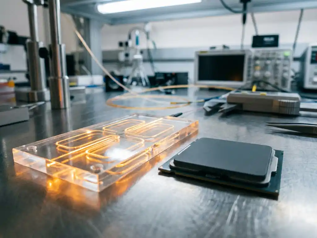
What are photonic chips and how do they work?
Photonic chips are specialized semiconductors that use light instead of electrons to process, transmit, and manipulate data. These photonic integrated circuits (PICs) contain multiple optical components on a single chip, including waveguides, modulators, and detectors, which control light signals for computing and communication tasks.
The fundamental operation of photonic chips differs significantly from that of traditional electronic processors. While electronic chips move electrons through silicon pathways, photonic chips guide photons through carefully designed optical waveguides. These light-based signals can carry far more information simultaneously across different wavelengths, similar to how fiber-optic cables transmit multiple data streams.
Photonic chip technology operates on three main platforms: indium phosphide (InP), silicon nitride (SiN), and silicon photonics (SiPh). Each platform offers distinct advantages for specific applications. InP enables direct light generation and advanced signal modulation, making it suitable for active optical components. SiN provides low propagation loss and compatibility with visible and near-infrared light, while SiPh offers high-volume manufacturing potential due to its compatibility with existing semiconductor fabrication processes.
The key benefits of photonic chips include high-speed data transmission, reduced power consumption, minimal signal loss and interference, and scalable manufacturing at lower cost. These advantages make integrated photonics a key enabling technology for applications requiring fast, efficient data processing and transmission.
Why would photonic chips be better than CPUs in smartphones?
Photonic chips could outperform traditional CPUs in smartphones primarily through dramatically reduced power consumption, faster data-processing speeds, and minimal heat generation. These advantages directly address the biggest limitations facing modern smartphone processors: battery life, thermal management, and performance bottlenecks.
Power efficiency represents the most significant advantage for mobile applications. Electronic CPUs generate substantial heat and consume considerable battery power when moving electrons through silicon pathways. Photonic chips, by contrast, use photons that do not interact with the chip material in the same way, resulting in much lower energy requirements for data transmission and processing. This efficiency gain could significantly extend smartphone battery life while maintaining or improving performance.
Speed advantages come from light’s inherent properties. Photons travel at the speed of light and can carry multiple data streams simultaneously across different wavelengths, enabling parallel-processing capabilities that surpass those of traditional electronic circuits. This means photonic chips could handle complex computational tasks, high-resolution displays, and real-time AI processing more efficiently than current CPUs.
Heat management becomes far less problematic with photonic chips since optical signals generate minimal thermal output compared with electronic switching. This reduction in heat generation allows for more compact designs, eliminates the need for extensive cooling systems, and prevents the thermal throttling that currently limits smartphone performance during intensive tasks.
The compact, scalable design of photonic chips also enables the integration of multiple optical components on a single chip, potentially reducing the overall size and complexity of smartphone internal components while increasing functionality.
What are the current limitations of photonic chips for mobile devices?
Current photonic chips face several significant limitations for smartphone applications, including the need for external light sources, larger component footprints than electronic circuits, integration challenges with existing electronic systems, and higher manufacturing costs for consumer-scale production.
Light-source integration presents the primary technical challenge. Most photonic chip platforms, particularly silicon nitride (SiN) and silicon photonics (SiPh), require external light sources such as lasers to function. Integrating these light sources into the compact form factor of a smartphone while maintaining efficiency and reliability remains a complex engineering challenge. While indium phosphide (InP) platforms can generate light directly, they face other limitations, including higher costs and material brittleness.
Size constraints create additional hurdles. Despite their advantages, many current photonic components require larger footprints than their electronic counterparts. Silicon nitride platforms, for example, typically require more area than silicon photonics, and both face challenges in achieving the miniaturization levels required for smartphone integration.
Manufacturing scalability and cost represent major barriers to consumer adoption. The specialized fabrication processes required for photonic chips currently cost more than traditional semiconductor manufacturing. While the PhotonDelta ecosystem and other industry initiatives are working to address scaling and industrialization challenges, achieving the cost levels necessary for mass-market consumer electronics remains a significant hurdle.
Integration complexity with existing smartphone architectures also poses challenges. Smartphones require seamless interaction among processors, memory, sensors, and communication systems. Developing hybrid systems that effectively combine photonic and electronic components while maintaining the reliability and performance standards consumers expect requires substantial engineering effort.
How close are we to photonic chips in consumer smartphones?
Consumer smartphones with photonic chip processors are likely still 10–15 years away from mainstream adoption, though specific photonic components may appear in premium devices within 5–7 years for specialized functions such as advanced sensing, high-speed data transmission, or AR/VR applications.
The current state of photonic chip technology places it in the early commercialization phase for specialized applications rather than general-purpose computing. The integrated photonics value chain is rapidly developing, with significant investments in research, manufacturing infrastructure, and application development. However, the transition from specialized industrial applications to consumer electronics requires overcoming substantial technical and economic challenges.
Industry progress indicators suggest a gradual integration approach. Photonic components will likely first appear in smartphones for specific functions where their advantages are most pronounced. Advanced biosensors using photonic chip technology could enable more accurate health monitoring in wearables and smartphones. High-speed optical transceivers might improve 6G connectivity and data-transfer capabilities.
The PhotonDelta ecosystem and similar global initiatives are accelerating development timelines through coordinated research, manufacturing infrastructure development, and industry collaboration. With over 300 partners spanning academia and industry, these efforts are addressing the scaling and industrialization challenges necessary for consumer applications.
Manufacturing readiness remains the critical factor determining adoption timelines. As photonic chip production scales and costs decrease, consumer applications become more feasible. Current projections suggest the photonic chip market could reach 300 million units by 2030 and over 1 billion by 2040, indicating substantial growth that could eventually include consumer electronics applications.
Which smartphone functions could benefit most from photonic technology?
Smartphone functions that could benefit most from photonic technology include camera systems and computational photography, biometric sensing and health monitoring, augmented reality (AR) applications, high-speed data connectivity, and AI processing tasks that require parallel computation.
Camera and imaging systems represent the most immediate opportunity for photonic integration. Advanced LiDAR-on-chip solutions could enable precise depth sensing, improved portrait-mode photography, and enhanced augmented reality experiences. Photonic chips can create compact, lightweight sensing solutions without moving parts, making them ideal for smartphone camera modules. These systems could provide real-time 3D mapping capabilities that surpass current smartphone depth-sensing technologies.
Health monitoring and biosensing applications offer significant potential for photonic integration. Photonic biosensors can enable accurate, point-of-care diagnostic capabilities directly in smartphones or connected wearable devices. These sensors could monitor various biomarkers reliably and cost-effectively while maintaining a small product footprint, transforming smartphones into comprehensive health-monitoring platforms.
Augmented reality functionality could see substantial improvements through photonic chip integration. PICs in AR applications enhance miniaturization and ergonomic design while enabling extremely clear vision with lower energy consumption. As smartphone AR capabilities expand, photonic chips could provide the processing power and display technologies necessary for seamless augmented reality experiences.
Connectivity and data transmission represent another area where photonic chips excel. High-speed optical transceivers using photonic chip technology could enable faster data transfer for both short-range and long-range optical communication in an energy-efficient manner. This capability becomes increasingly important as 5G and future 6G networks demand higher data throughput and lower latency.
AI processing tasks requiring parallel computation could benefit from photonic chips’ ability to process multiple data streams simultaneously across different wavelengths. This parallel-processing capability could accelerate machine-learning inference, real-time language translation, and computational photography algorithms while consuming less power than traditional electronic processors.
The journey toward photonic chips in smartphones represents more than just technological evolution—it signals a fundamental shift in how we approach mobile computing. While complete CPU replacement may still be years away, the gradual integration of photonic components into specific smartphone functions offers a glimpse into a future where light-based processing transforms our mobile experience. The collaborative efforts within the global ecosystem are steadily addressing manufacturing challenges and scaling limitations, while strategic funding initiatives accelerate research and development timelines. As the industry continues developing specialized human capital and expanding internationalization efforts, the convergence of optical and electronic technologies promises to unlock new possibilities in mobile computing that could redefine how we interact with our devices in the coming decades.