Understanding the fundamental differences between active and passive photonic chips is essential for anyone exploring integrated photonics. These two types of Photonic Integrated Circuits (PICs) serve complementary but distinct roles in modern optical systems, from high-speed data communications to advanced sensing applications.
Active photonic chips generate and manipulate light using electrical energy, while passive components guide and modify existing light signals without requiring external power. Together, they form the foundation of photonic chip technology, enabling breakthrough solutions across industries ranging from telecommunications to healthcare diagnostics.
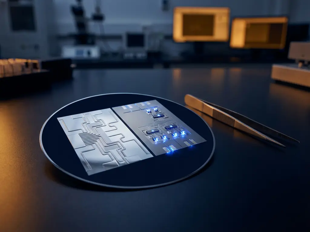
What are active and passive photonic chips?
Active photonic chips contain components that generate, amplify, or modulate light using electrical energy, while passive photonic chips manipulate existing light signals through structures that require no external power source. Both types work together in integrated photonics systems to create complete optical solutions.
Active components include lasers, optical amplifiers, modulators, and photodetectors. These elements convert electrical signals to optical signals, or vice versa, making them essential for generating and detecting light within photonic systems. They require electrical power to operate and can actively change the properties of light passing through them.
Passive components include waveguides, splitters, combiners, filters, and resonators. These structures guide light along predetermined paths, split or combine optical signals, and filter specific wavelengths without consuming power. They rely on physical geometry and material properties to manipulate light rather than external energy sources.
The distinction between active and passive elements mirrors similar concepts in electronic circuits, where active components like transistors require power while passive elements like resistors and capacitors do not. In integrated photonics, this fundamental difference determines how each component type contributes to overall system functionality.
How do active photonic chips generate and control light?
Active photonic chips generate light through semiconductor laser diodes that convert electrical current into photons via stimulated emission. They control light properties by using electrical signals to modulate the intensity, phase, frequency, or polarization of optical signals in real time.
Laser sources within active chips typically use direct-bandgap semiconductor materials such as indium phosphide (InP), which efficiently convert electrical energy into light. When current flows through the laser diode, electrons combine with holes in the semiconductor material, releasing energy as photons. This process enables precise control over wavelength and output power.
Optical modulators are another crucial active component for controlling existing light signals. These devices use electric fields to change the refractive index of materials, enabling rapid switching or modulation of optical signals. Electro-optic modulators can operate at speeds exceeding 100 GHz, enabling high-speed data transmission applications.
Photodetectors complete the active component family by converting optical signals back into electrical signals. These devices absorb photons and generate an electrical current proportional to the incident optical power, enabling signal detection and measurement within photonic systems.
What functions do passive photonic chips perform?
Passive photonic chips route, split, combine, and filter light signals using precisely engineered structures that manipulate optical properties through geometry and material characteristics. These components provide the optical interconnect infrastructure that connects active elements within integrated photonics systems.
Waveguides are the fundamental passive component, acting as optical highways that confine and direct light along specific paths on the chip. These structures use the principle of total internal reflection, similar to optical fibers, to guide light with minimal loss across the photonic circuit.
Optical splitters and combiners enable signal distribution and aggregation within photonic systems. Splitters divide a single optical signal into multiple outputs, while combiners merge multiple signals into a single output. These components are essential for creating complex on-chip optical networks.
Wavelength filters and resonators provide spectral control by selectively transmitting or reflecting specific wavelengths. Ring resonators, for example, can isolate narrow wavelength bands for wavelength-division multiplexing applications, while Bragg gratings provide precise spectral filtering.
What’s the difference between manufacturing active vs. passive photonic chips?
Manufacturing active photonic chips requires complex epitaxial growth processes and precise doping to create semiconductor junctions, while passive components use simpler fabrication techniques focused on etching and depositing dielectric materials to achieve the desired optical properties.
Active component fabrication typically involves growing multiple semiconductor layers with different compositions and doping levels. For InP-based active chips, molecular beam epitaxy or metal-organic chemical vapor deposition creates the precisely controlled layer structures needed for laser operation and optical gain.
The manufacturing process for active components also requires specialized steps such as contact metallization for electrical connections and facet preparation for optical coupling. These additional processing steps increase complexity and cost compared with passive component fabrication.
Passive component manufacturing focuses primarily on lithographic patterning and etching to create the desired waveguide geometries. Silicon nitride (SiN) and silicon photonics (SiPh) platforms use established semiconductor fabrication techniques, making them more compatible with existing foundry infrastructure and enabling lower-cost, high-volume production.
How are active and passive components integrated in photonic systems?
Active and passive components are integrated through hybrid or heterogeneous approaches that combine different material platforms on a single chip or within a single package. This integration leverages the strengths of each platform while addressing the diverse requirements of modern photonic applications.
Hybrid integration involves manufacturing active and passive chips separately and then combining them at the packaging level through precise optical alignment and coupling. This approach allows each component type to be optimized using its ideal material platform while maintaining design flexibility for complex systems.
Heterogeneous integration creates monolithic solutions by directly bonding or growing active materials onto passive substrates. This technique enables tighter integration and potentially lower costs for high-volume applications, though it requires more sophisticated manufacturing capabilities.
The PhotonDelta ecosystem supports both integration approaches through its comprehensive integrated photonics value chain, spanning design, fabrication, packaging, and testing. This end-to-end capability enables the development of sophisticated photonic systems that combine multiple platforms to address increasingly complex application requirements across industries such as telecommunications, healthcare, and automotive sensing.
As the integrated photonics field continues to evolve, the synergy between active and passive photonic chips becomes increasingly important for developing next-generation optical systems. The manufacturing complexity of these components drives the need for specialized human capital with deep expertise in both optical design and semiconductor fabrication. Companies looking to enter this space often benefit from exploring funding opportunities that support the development of integrated photonic solutions. The collaborative nature of this technology also highlights the value of participating in a robust ecosystem where knowledge sharing and partnership opportunities accelerate innovation. For organizations considering expansion into global markets, understanding the internationalisation landscape can provide valuable insights into regional market dynamics and regulatory considerations that shape the deployment of photonic technologies worldwide.