The underwater environment presents unique challenges for electronic systems, but photonic chips offer promising solutions for marine applications. As integrated photonics technology advances, engineers are exploring how these light-based semiconductors can function in aquatic conditions where traditional electronics often fail.
Photonic integrated circuits (PICs) use photons instead of electrons to process and transmit information, making them fundamentally different from conventional electronic chips. This difference creates new possibilities for underwater sensing, communication, and monitoring systems that could transform marine research and ocean exploration.
What are photonic chips, and how do they work in water?
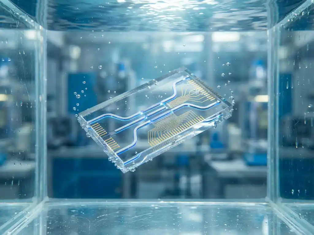
Photonic chips are semiconductor devices that use photons instead of electrons to process and transmit information. Underwater, these chips can operate via fiber-optic connections and specialized packaging that protects the photonic components while allowing optical signals to pass through.
The core advantage of photonic chip technology in aquatic environments stems from light’s ability to travel through water more effectively than electrical signals in many applications. While water conducts electricity and can cause short circuits in electronic systems, properly designed photonic systems can maintain signal integrity through optical transmission.
Photonic chips combine multiple optical components on a single substrate, including waveguides, modulators, and detectors. When deployed underwater, these components must be housed in waterproof enclosures, but the optical signals themselves can interface with the water environment through specialized optical windows or fiber-optic cables. This design approach enables underwater sensing applications in which the photonic chip remains protected while still interacting with the marine environment.
Can photonic chips survive underwater conditions?
Photonic chips can survive underwater conditions when properly packaged and sealed, much like electronic components used in marine environments. The photonic components themselves are not inherently waterproof, but specialized packaging techniques enable their deployment in aquatic applications.
The survival of photonic chips underwater depends on several critical factors. Pressure resistance is essential for deep-water applications, requiring robust housing materials that can withstand increasing water pressure without compromising the optical pathways. Corrosion protection is equally important, as saltwater environments can degrade metal components and connections over time.
Temperature stability also plays a crucial role, as underwater environments can experience significant temperature variations. Photonic chips must maintain their optical properties across these ranges to ensure reliable operation. Packaging materials and sealing methods must account for thermal expansion and contraction while maintaining watertight integrity.
Modern packaging solutions for underwater photonic systems include ceramic housings, specialized optical feedthroughs, and hermetic sealing techniques. These approaches have proven effective in existing underwater optical communication systems and scientific instruments that rely on photonic components.
What are the main applications of photonic chips underwater?
The main underwater applications for photonic chips include optical communication systems, environmental monitoring sensors, underwater LiDAR for mapping, and biosensing platforms for marine research. These applications leverage the unique advantages of integrated photonics in aquatic environments.
Underwater optical communication is one of the most developed applications. Photonic chips enable high-speed data transmission between submarines, underwater vehicles, and surface platforms through blue-green laser communication systems. These systems can achieve higher data rates than traditional acoustic communication methods while offering security advantages.
Environmental sensing applications use photonic biosensors for real-time water-quality monitoring. These lab-on-a-chip platforms can detect pollutants, measure pH, monitor dissolved oxygen, and identify biological markers in marine environments. The compact nature of photonic chip technology makes these sensors suitable for deployment on autonomous underwater vehicles or fixed monitoring stations.
Underwater mapping and navigation systems benefit from photonic-based LiDAR technology. These compact sensors can create detailed three-dimensional maps of underwater terrain, coral reefs, and marine structures. The precision and reliability of photonic chips make them valuable for scientific research, underwater construction, and marine archaeology.
How do underwater photonic systems compare to traditional electronics?
Underwater photonic systems offer superior signal integrity and reduced power consumption compared with traditional electronics, but they require more complex packaging and higher upfront costs. The comparison depends on the specific application and deployment requirements.
Signal transmission is a key advantage for photonic systems. While electrical signals can suffer from interference and attenuation in conductive seawater, optical signals maintain their quality over longer distances. This characteristic makes photonic systems particularly valuable for long-range underwater communication and sensing.
Power efficiency is especially important in underwater deployments where battery replacement is difficult or impossible. Photonic chips typically consume less power than comparable electronic systems, extending operational lifetimes for autonomous underwater platforms. This efficiency advantage becomes more significant as system complexity increases.
However, traditional electronics often allow simpler integration and lower costs for basic underwater applications. Electronic systems have established supply chains and well-understood packaging techniques for marine environments. The choice between photonic and electronic solutions depends on performance requirements, deployment duration, and application-specific cost considerations.
What challenges do engineers face with underwater photonics?
Engineers face several primary challenges, including optical-window fouling, pressure-resistant packaging design, thermal management, and maintaining optical alignment in dynamic underwater environments. These technical hurdles require specialized solutions beyond standard photonic chip design.
Biofouling presents a persistent challenge for underwater optical systems. Marine organisms can accumulate on optical windows and surfaces, degrading system performance over time. Engineers must develop antifouling coatings and cleaning mechanisms to maintain optical clarity throughout deployment.
Packaging complexity increases significantly for underwater applications. Standard photonic chip packaging methods must be adapted to handle water pressure, corrosion, and mechanical stress while preserving optical performance. This requirement often leads to larger, more expensive packaging solutions that can limit deployment options.
The PhotonDelta ecosystem addresses some of these challenges through its integrated photonics value chain, which includes specialized packaging and testing capabilities. However, underwater applications remain a developing area, and continued research and development focus on improving reliability and reducing costs for marine photonic systems.
Optical alignment stability poses another significant challenge, as underwater currents and vibrations can affect the precise positioning required for optimal photonic system performance. Engineers must design robust mounting systems and may need to incorporate active alignment-correction mechanisms to maintain functionality in dynamic marine environments.
As underwater photonics continues to mature, the field presents exciting opportunities for engineers and researchers willing to tackle these complex challenges. The growing ecosystem of integrated photonics companies is developing specialized solutions that could revolutionize marine technology. Success in this domain requires not only technical expertise in photonic chips but also access to specialized human capital with marine engineering experience. Organizations pursuing underwater photonic applications often benefit from collaborative approaches and targeted funding opportunities that support both fundamental research and practical deployment challenges. The intersection of photonics and marine technology represents a frontier where interdisciplinary collaboration and internationalization efforts can accelerate progress toward more capable underwater systems.