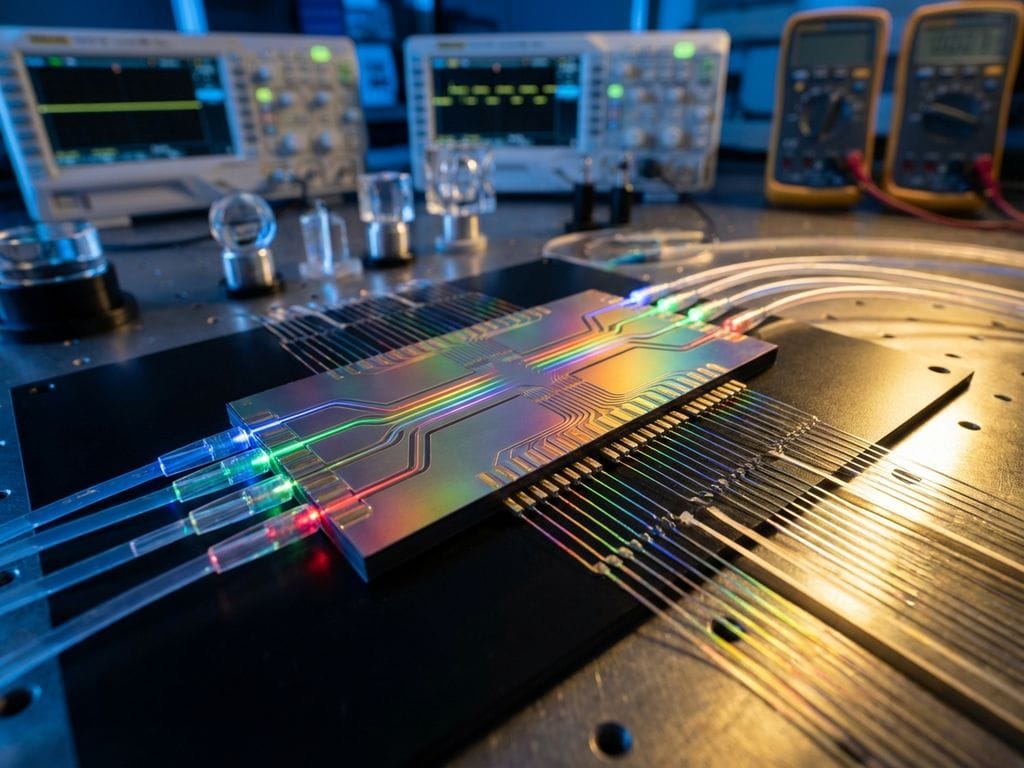
Photonic chips offer significant speed advantages over traditional electronic semiconductors by processing data at the speed of light rather than relying on electron movement. These chips can handle data transmission rates exceeding 100 gigabits per second while consuming substantially less power. The speed benefits stem from light-based signal transmission, reduced electromagnetic interference, and superior parallel processing capabilities that eliminate electronic bottlenecks in data handling.
How fast can photonic chips actually process data compared to electronic chips?
Photonic chips process data at fundamentally faster speeds than electronic chips because they use light photons instead of electrons for signal transmission. While electronic chips are limited by electron mobility and resistance, photonic chips operate at light speed through optical waveguides, enabling data rates that can exceed 100 gigabits per second in practical applications.
The speed difference becomes particularly pronounced in data transmission applications. Electronic chips face increasing challenges as data rates climb due to signal degradation, power consumption, and heat generation. Photonic Integrated Circuits (PICs) maintain signal integrity across longer distances without the same performance penalties.
In telecommunications infrastructure, photonic chips demonstrate their speed advantages through high-capacity optical transceivers. These devices can simultaneously handle multiple wavelengths of light, each carrying separate data streams, effectively multiplying the total data throughput. This wavelength-division multiplexing capability allows a single photonic chip to process terabits of data per second.
The fundamental physics behind this speed advantage lies in the properties of light versus electrical signals. Light travels at approximately 300 million metres per second in a vacuum and maintains high speeds even through optical materials. Electronic signals, by contrast, face resistance, capacitance, and inductance that slow transmission and create delays in processing chains.
What makes photonic chips so much faster than traditional semiconductors?
Photonic chips achieve superior speed through light-based signal transmission that eliminates many physical limitations affecting electronic semiconductors. Light signals do not experience electrical resistance, electromagnetic interference, or the capacitive delays that constrain electronic circuits, enabling faster data processing and transmission.
The absence of electromagnetic interference represents a crucial advantage for photonic chip technology. Electronic circuits generate electromagnetic fields that can interfere with neighbouring components, requiring careful shielding and spacing that limit miniaturisation and speed. Photonic signals remain isolated within optical waveguides, preventing crosstalk and allowing denser integration without performance degradation.
Parallel processing capabilities further enhance photonic chip speed advantages. Multiple wavelengths of light can travel simultaneously through the same optical pathway, each carrying independent data streams. This wavelength-division approach enables massive parallel processing that would require multiple electronic pathways to achieve equivalent throughput.
The integrated photonics value chain benefits from reduced power consumption at high speeds. Electronic chips require increasing power to drive faster switching speeds, generating heat that further limits performance. Photonic chips maintain efficiency across wider speed ranges, supporting sustained high-performance operation without thermal throttling.
Silicon nitride (SiN) and indium phosphide (InP) platforms each contribute specific speed advantages. SiN platforms offer low-propagation-loss waveguides that maintain signal quality across longer distances, while InP platforms enable direct light generation and advanced signal modulation for complex high-speed applications.
Which applications benefit most from photonic chip speed advantages?
Data centres and telecommunications infrastructure gain the most significant benefits from photonic chip speed advantages, requiring high-speed optical transceivers to handle exponentially growing data consumption demands. These applications need sustained high-bandwidth performance that electronic solutions struggle to provide efficiently.
Autonomous vehicle systems represent another transformative application area. Optical LIDAR systems built with photonic chips can process environmental data at speeds necessary for real-time decision-making in autonomous driving scenarios. The automotive sector, representing over 7% of EU GDP, increasingly relies on photonic solutions for safety-critical sensing applications.
High-performance computing applications leverage photonic chip speed for interconnects between processors and memory systems. As computing demands increase, the bottleneck shifts from processing power to data movement speed. Photonic interconnects eliminate many electronic communication limitations, enabling faster system-wide performance.
Quantum computing systems benefit from photonic chip precision and speed for quantum state manipulation and measurement. The ability to process optical signals with minimal noise and maximum speed supports the delicate operations required for quantum information processing.
Healthcare applications utilise photonic chip speed advantages in point-of-care (PoC) platforms for rapid diagnostic testing. Medical sensing applications require fast, accurate analysis of biomarkers, where photonic chips enable miniaturised devices with high accuracy and low cost for decentralised healthcare solutions.
Consumer electronics, particularly wearables, benefit from photonic chips’ ability to create fully integrated sensing solutions. These devices can monitor multiple biomarkers simultaneously while maintaining small product footprints and extended battery life through efficient optical processing.
What are the current limitations of photonic chip speed performance?
Manufacturing complexity represents the primary limitation constraining photonic chip speed performance. Unlike mature electronic semiconductor processes, integrated photonics manufacturing requires specialised fabrication techniques and materials that are more challenging to produce consistently at scale, affecting both performance reliability and cost-effectiveness.
Integration challenges with electronic systems create practical speed bottlenecks. Most applications require hybrid solutions combining photonic and electronic components. The interfaces between these different technologies can introduce delays and complexity that partially offset pure photonic speed advantages.
Silicon nitride (SiN) and silicon photonics (SiPh) platforms both require separate light sources to be integrated, adding complexity to system design. This integration requirement can introduce additional components that impact overall system speed and reliability compared to platforms like indium phosphide (InP) that enable direct light generation.
Power consumption considerations vary across different photonic platforms. While photonic chips generally consume less power than electronic alternatives at high speeds, some applications still require electronic control circuits and optical amplifiers that can impact overall system efficiency.
Material limitations affect different platforms in specific ways. Indium phosphide offers excellent optical properties but faces higher propagation losses and material costs. The brittle nature of indium limits wafer sizes, affecting manufacturing scalability compared to silicon-based alternatives.
Standardisation challenges slow adoption and limit speed optimisation. The photonic chip industry remains in the early stages of development, with limited Process Design Kits (PDKs) and standardised design libraries compared to mature electronic semiconductor ecosystems. This affects design cycle times and limits the ability to optimise for maximum speed performance across different applications.
Current photonic chip technology delivers substantial speed advantages over electronic alternatives, particularly in data transmission, telecommunications, and sensing applications. The fundamental physics of light-based processing enables performance levels that electronic systems cannot match efficiently. However, manufacturing complexity, integration challenges, and standardisation requirements continue to constrain widespread adoption. As the ecosystem matures and addresses these limitations, the development of photonic chips will likely accelerate through enhanced human capital development and strategic funding initiatives. The growing focus on internationalisation will also play a crucial role in establishing photonic chips as essential components in applications demanding maximum speed and efficiency across global markets.