Heterogeneous integration key to future integrated-photonics growth
31 August 2021No single integrated-photonics technology can do it all: they need to be combined for maximum functionality. The set of techniques to do that – hybrid or heterogeneous integration – is a key growth driver for the Dutch integrated-photonics industry. This article explains what heterogeneous integration is and why it matters.
In electronics, the vast majority of chips are based on silicon. Other semiconductor materials are preferred only for specialized applications. In power management chips, for example, gallium nitride (GaN) is an up-and-coming substrate. But although emerging applications such as electric driving will certainly spur demand for GaN chips over the next few years, it’s unlikely they’ll ever challenge silicon’s crown in terms of number of chips manufactured or revenue generated.
The situation isn’t as clear-cut in integrated photonics. Each of the three main ‘flavors’ of this technology – indium phosphide (InP), silicon nitride (SiN) and silicon/silica photonics (SiP) – has its own strengths and weaknesses. Rather than thinking about these platforms as competing with one another, they should be considered complementary. For many applications, any one platform can’t shine without the other: they need to be combined to unlock certain functionality. Boosting performance or lowering cost can also be an incentive to making combinations.
What is hybrid or heterogeneous integration (HI)?
Integration of separately manufactured components into higher-level assemblies is called hybrid or heterogeneous integration (HI). Apart from blending photonic flavors, HI is indispensable because all but the most simple photonic devices require control electronics to operate. The optical and electronic chips are manufactured in their own respective factories and then connected, assembled and packaged together into one module.
As the integrated-photonics industry matures, photonic devices will perform increasingly complex tasks. This will likely involve assembling a growing number of components, using increasingly sophisticated HI techniques. These components aren’t just photonic integrated circuits (PICs) and control chips but other (discrete) components as well. Eventually, more ‘exotic’ devices such as MEMS and (bio)sensors will make their way in there.
The key to growth of the integrated photonics industry
Aspiring to become a worldwide focal point of the integrated photonics industry, it therefore comes as no surprise that the Dutch Photondelta ecosystem is preparing for HI to gain ground. “We’re currently working out what our businesses need both in the near future and beyond. Next, we intend to set up R&D programs to accelerate development of HI technology. Accelerating the growth of the Dutch photonics industry is the reason Photondelta was founded, and we believe HI will be key to sustain healthy growth rates in the future,” says Carol de Vries, program manager at Photondelta.
The advantages of combining different production platforms
Indium phosphide (InP) is the only integrated-photonics platform that allows for the integration of active components such as lasers, amplifiers, photodetectors and modulators. If an active component is needed in a silicon nitride (SiN) or silicon photonics (SiP) PIC – and at the very least they need a light source – either a discrete component will need to be connected or it will need to be integrated with an InP chip.
Still, there are very good reasons to work with SiN or SiP. The former operates in a broad wavelength range, enabling unique applications, and features relatively low light losses, enabling more extended circuitry. SiP isn’t quite as good as SiN as far as those characteristics are concerned, but it can be manufactured cheaply and in high volumes with the same CMOS processes used to manufacture ICs.
In theory, a single process could be developed in which all three materials come together to create the ultimate PICs. In practice, that’s a pipe dream, explains Albert Hasper, CEO of photonics assembly foundry Phix. “That would only work at extremely high volumes. Integrated photonics is growing rapidly, but it’s not even close to the required numbers and it won’t get there anytime soon, if ever.”
“It wouldn’t make much sense economically,” Hasper continues. “Say, for example, a SiN PIC needs a photodetector, which is a very small component compared to the actual circuit. You could either have it made cheaply in a CMOS process and use HI to place the unit on the SiN PIC, or you could manufacture it alongside the circuit using the hypothetical all-in-one process, which would require many additional process steps for a component that takes up a very small part of the chip’s surface. Clearly, at this moment, HI is more cost effective. It’s the most flexible option, too. Generally, HI provides the opportunity to get the best of both worlds.”
Beyond its intrinsic benefits, De Vries adds, HI is how the Photondelta ecosystem can connect with the rest of the integrated-photonics world, SiP in particular. “We don’t have SiP activities here: it’s manufactured by large semiconductor foundries such as Globalfoundries and TSMC. Our companies specialize in InP and SiN PICs, but at some point, it might become interesting to do designs in SiP as well. Conversely, SiP companies likely want to take advantage of our InP and SiN technology. We need to build bridges between these worlds, and HI is the way to do it.”
What are PHIX’ experiences with hybrid integration?
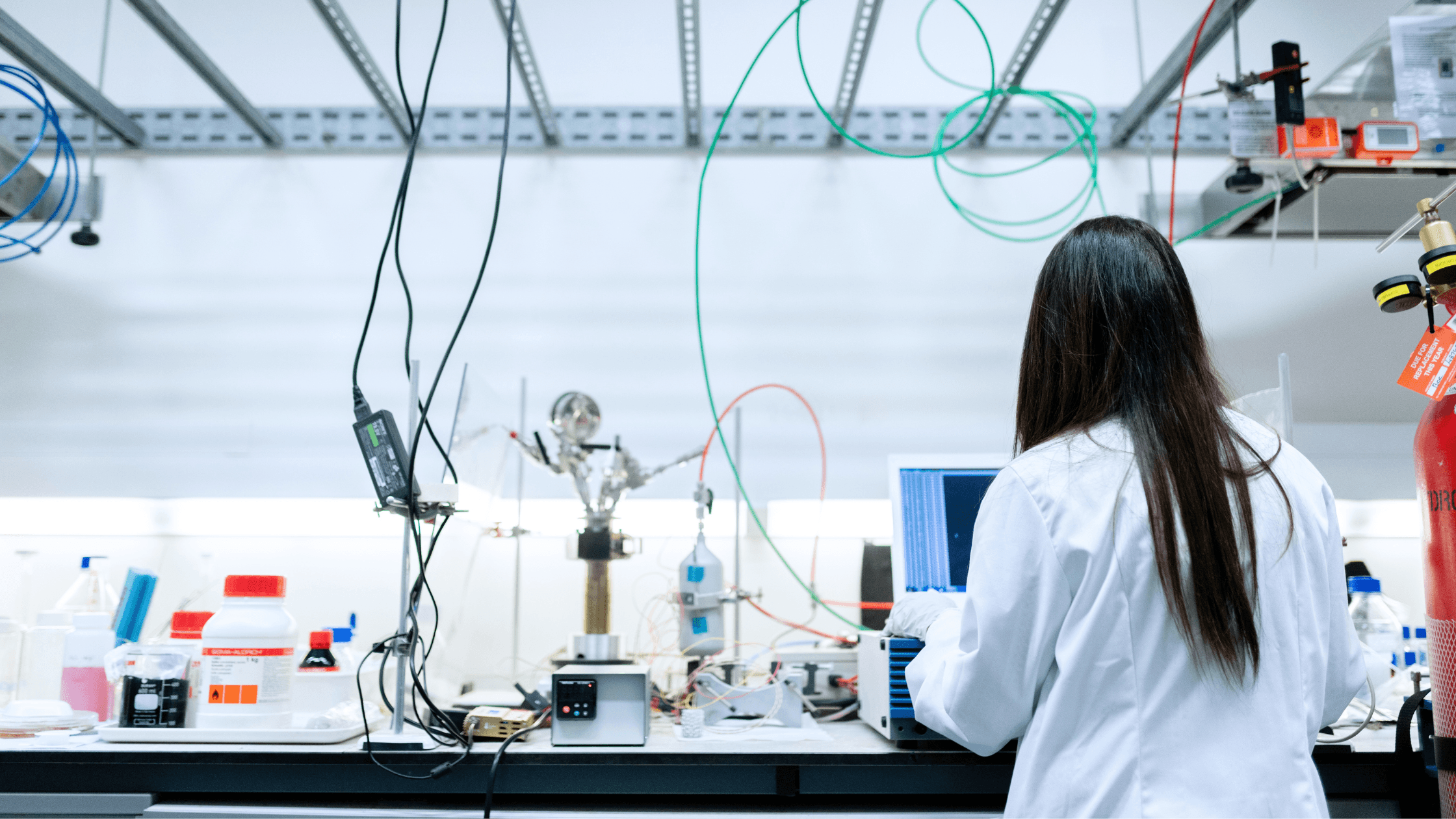
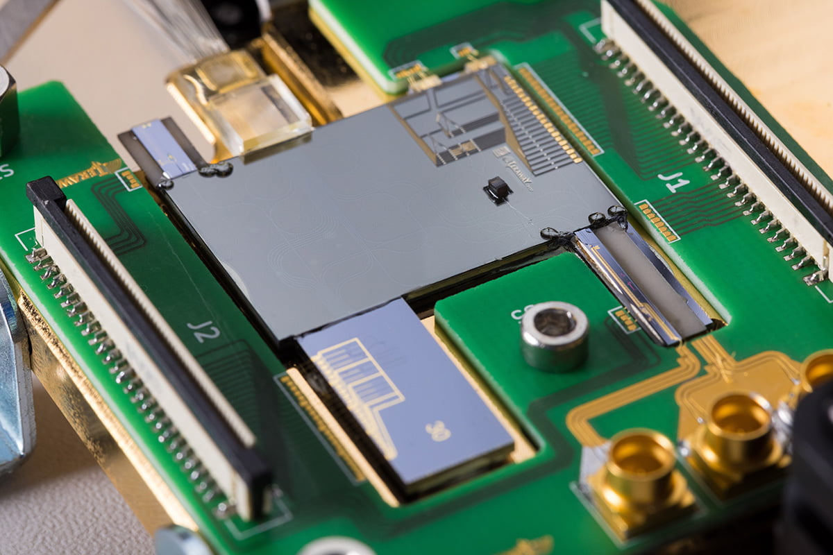
HI is already daily routine at Hasper’s assembly and packaging facility in Enschede, which houses equipment to either flip-chip dies on top of each other or join them at the edges (allowing the light to stay in-plane). Both processes require very high-accuracy manufacturing steps, as even the slightest misalignment can cause loss of precious light. The speed of the process is an important issue, too, of course.
“We assemble and combine different platforms for a lot of customers. Currently, the development of these products is still in the prototype and medium-volume stage. Our semi-automatic assembly line can handle the next phase, featuring volumes up to a few thousand units per month, but we’re not ready yet to scale up towards very high volumes. From my perspective, this is the next HI bottleneck: getting the equipment and industrial automation sorted for that phase. This is a great opportunity for the Dutch equipment manufacturing sector, actually.” Hasper notes that to get to these high volumes, also InP and SiN PIC manufacturing capacity needs to increase.

The advantage of HI for tranceivers
Another Dutch photonics company that’s already getting its hands dirty in HI is Effect Photonics, which is commercializing optical transceivers for telecom and datacom markets. “For us, the HI of optics and electronics is very important to deal with the high data rates,” says president Boudewijn Docter. “As data rates increase, the electrical connections need to get shorter. We’re currently working with data rates of 25 Gb/s and higher, for which a few millimeters are challenging. That’s why we need the integration of the photonic and electronic chips to be as intimate as possible – at least where the high-speed connections are concerned. We’ll initially still use traditional wire bonds, but we’re definitely looking into flip-chipping and more advanced types of vertical integration for our next-generation products.”
For another component, for which the length of the electrical connection wasn’t as critical, stacking it on top of the InP PIC turned out to be the best solution for a very practical reason, Docter continues. “The component had to be positioned right where the fiber-optic connector is. So, there simply wasn’t any room physically to put the component next to the chip. We basically had no other choice than to put it on top.”

Integration techniques and considerations
While Docter suspects that the photonics industry will embrace more and more HI techniques as the complexity of the products grows, he adds that applying HI will always be the result of carefully weighing functionality, (overall) cost and performance – it’s not a panacea. “In addition, most companies want to stay away from risky experiments. They’ll only employ techniques that have proven themselves in extensive reliability and stress tests.”
Fortunately, the integrated-photonics sector has the semiconductor industry to pull the chestnuts from the fire. Previously, the former already ‘borrowed’ basic integration techniques such as wire bonding and flip-chipping. As chipmakers step up their efforts to develop more advanced integration and packaging techniques, some of these may be useful in integrated photonics as well. Incidentally, chipmakers’ interest in integrated photonics is growing fast, for example, to replace copper wires for intra- and inter-chip communication. That would obviously involve advanced HI as well.
However, HI techniques developed for semiconductors can’t be copied one-on-one to integrated photonics, De Vries warns. “The component density of PICs is much lower than that of advanced CMOS because photonic structures are comparatively large. This means that some HI options may be technically possible but not cost effective because of the big size difference of the chips.”
Physics can get in the way, too, De Vries continues. “InP and Si, for example, have different thermal expansion coefficients. This generates mechanical stress when two dies of these materials are stacked, which needs to be mitigated. This can be accomplished, for example, using interposers, a kind of intermediary layers.”
And, finally, there are practical considerations. “Optical connections require much more accurate alignment than what’s commonly needed in the semiconductor industry, and fixation has different requirements. This is especially the case with edge-to-edge connections. Emitting light out-of-plane, on the other hand, requires gratings or mirrors, which are large and hard to produce on-chip.”
“In case of wafer-scale integration, it’s important to note that InP is manufactured on 75 mm, 100 mm and in the future perhaps 150 mm wafers, whereas the standard for Si and SiN is 200 mm and 300 mm. So InP/SiN or InP/Si wafer-scale integration requires special bonding strategies. It’s possible to mount InP coupons on Si or SiN, though.”
De Vries expects that relatively straightforward multi-chip and system-in-package solutions, which have been applied in the semiconductor industry for ages, will be preferred for most applications while volumes are still relatively low. “It’s imperative, however, that we keep up with worldwide developments in HI. It’s how the companies in the Photondelta ecosystem expand their possibilities and markets.” Docter agrees: “We’ll become much more interesting to the rest of the world by offering the right interfaces to our technology.”
This article was written in close collaboration with Bits & Chips Magazine.